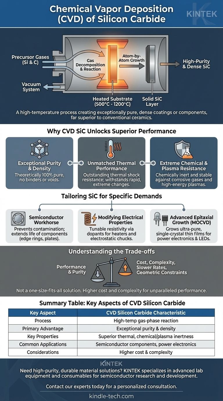
In essence, the chemical vapor deposition (CVD) of silicon carbide is a high-temperature manufacturing process used to create exceptionally pure and dense silicon carbide coatings or solid components. It works by introducing volatile precursor gases containing silicon and carbon into a vacuum chamber, where they react and decompose on a heated surface, building up a solid SiC layer atom by atom. This method produces a material with performance characteristics far superior to those of SiC made by conventional ceramic processes.
The critical takeaway is that CVD is not just another way to make silicon carbide; it is a specialized technique that engineers a material with near-perfect purity and structure. This makes CVD SiC an enabling material for extreme-environment applications, particularly in semiconductor manufacturing, where typical ceramics would fail.
Deconstructing the CVD Process
To understand the value of CVD silicon carbide, you must first understand the precision of the process itself. It is a synthesis method built from the ground up, not a refinement of a pre-existing material.
The Core Ingredients and Environment
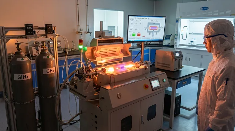
The process begins with a carefully controlled set of inputs. This includes one or more precursor gases that contain the necessary silicon and carbon atoms. These gases are injected into a reaction chamber under a strong vacuum.
The chamber also contains the object to be coated, known as the substrate, which is heated to a very high temperature, often between 500°C and 1200°C.
The Deposition and Growth Mechanism
At these high temperatures, the precursor gases become unstable and decompose when they come into contact with the hot substrate. This chemical reaction breaks the molecular bonds, freeing the silicon and carbon atoms.
These freed atoms then bond with each other directly on the substrate's surface, forming a new, solid layer of silicon carbide. Over time, this layer grows in a highly uniform and controlled manner, creating a dense, non-porous coating or even a freestanding part.
Why CVD Unlocks Superior Performance
The properties of the final material are a direct result of this bottom-up synthesis. The CVD process is chosen when standard ceramic fabrication methods are insufficient for the application's demands.
Exceptional Purity and Density
Unlike traditional ceramics made from powders (like recrystallized SiC), which often contain binders and inherent porosity, CVD SiC is theoretically 100% pure. This lack of impurities and voids is critical for predictable performance in sensitive environments.
Unmatched Thermal Performance
CVD SiC exhibits outstanding thermal shock resistance. It can withstand rapid and extreme temperature changes without cracking, making it ideal for components in rapid thermal processing (RTP) chambers used in semiconductor fabrication.
Extreme Chemical and Plasma Resistance
The material is chemically inert and physically stable. This allows it to resist erosion from the highly corrosive gases and high-energy plasmas used in semiconductor etch chambers. This same stability makes it suitable for components like desulfurization nozzles in industrial power plants.
Tailoring SiC for Specific Demands
A key advantage of the CVD process is the ability to tune the material's properties for specific functions, moving beyond a one-size-fits-all approach.
The Semiconductor Workhorse
The primary application for CVD SiC is in semiconductor processing. Its purity prevents contamination of silicon wafers, while its durability extends the life of critical chamber components like edge rings, gas distribution plates, and liners.
Modifying Electrical Properties
By introducing specific dopant gases during the CVD process, the electrical resistivity of the silicon carbide can be precisely controlled. This allows it to be engineered as a conductor for applications like heaters and electrostatic chucks, which hold wafers in place using an electric field.
Advanced Epitaxial Growth (MOCVD)
A specialized variant called Metal-Organic Chemical Vapor Deposition (MOCVD) is used to grow ultra-pure, single-crystal thin films of SiC. This level of crystalline perfection is essential for fabricating high-performance semiconductor devices themselves, such as power electronics and bright LEDs.
Understanding the Trade-offs
While CVD SiC offers unparalleled performance, it is not the solution for every problem. The choice to use it involves clear trade-offs.
Cost and Complexity
CVD requires sophisticated vacuum systems, high-purity precursor gases, and significant energy input. This makes it a considerably more expensive and complex process compared to traditional methods like sintering powdered SiC.
Slower Deposition Rates
Building a thick, solid component via CVD is a time-consuming process. The layer-by-layer growth can be slow, making it less economical for producing large, bulky parts where ultimate purity is not the primary concern.
Geometric Constraints
The process relies on gas reaching a uniformly heated surface. Coating highly complex internal geometries or shielded areas can be challenging, potentially leading to non-uniform thickness or coverage.
Making the Right Choice for Your Goal
Selecting the correct form of silicon carbide depends entirely on your application's specific technical and commercial requirements.
- If your primary focus is maximum purity and performance in extreme environments: CVD silicon carbide is the definitive choice for applications like semiconductor plasma etch or high-temperature chemical processing.
- If your primary focus is general high-temperature structural components: For applications like kiln furniture or heat exchangers where some porosity is acceptable and cost is a driver, other forms like recrystallized or sintered SiC may be more suitable.
- If your primary focus is fabricating next-generation electronic devices: Specialized epitaxial CVD methods like MOCVD are non-negotiable for creating the required single-crystal SiC substrates and layers.
Ultimately, understanding the CVD process is the key to unlocking silicon carbide's full potential for the world's most demanding technical challenges.
Summary Table:
| Key Aspect | CVD Silicon Carbide Characteristic |
|---|---|
| Process | High-temperature gas-phase reaction building material atom-by-layer |
| Primary Advantage | Exceptional purity and density, free from binders and porosity |
| Key Properties | Superior thermal shock resistance, extreme chemical/plasma inertness |
| Common Applications | Semiconductor chamber components (edge rings, heaters), power electronics, LEDs |
| Considerations | Higher cost and complexity vs. traditional ceramic methods |
Need a high-purity, durable material solution for your most demanding applications?
The CVD silicon carbide process is engineered for extreme performance where standard materials fail. At KINTEK, we specialize in providing advanced lab equipment and consumables, including solutions for high-performance materials like SiC. Our expertise can help you select the right components for semiconductor manufacturing, research, and development.
Let's discuss how our products can enhance your laboratory's capabilities. Contact our experts today for a personalized consultation.
Visual Guide
Related Products
- Silicon Carbide (SIC) Ceramic Sheet Wear-Resistant Engineering Advanced Fine Ceramics
- Silicon Carbide (SIC) Ceramic Plate for Engineering Advanced Fine Ceramics
- Silicon Carbide (SIC) Ceramic Sheet Flat Corrugated Heat Sink for Engineering Advanced Fine Ceramics
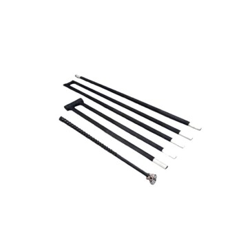
- Silicon Carbide SiC Thermal Heating Elements for Electric Furnace
- CVD Diamond for Thermal Management Applications
People Also Ask
- What is the temperature resistance of silicon carbide? Withstands Extreme Heat Up to 1500°C
- What are the properties and applications of silicon carbide ceramics? Solve Extreme Engineering Challenges
- Why is silicon carbide more efficient? Unlock Higher Power Density with SiC's Superior Material Properties
- What are the common uses of silicon carbide? Unlock Extreme Performance in Harsh Environments
- What is the process of making silicon carbide? From Raw Materials to Advanced Ceramics