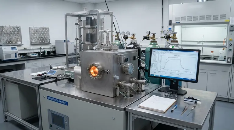
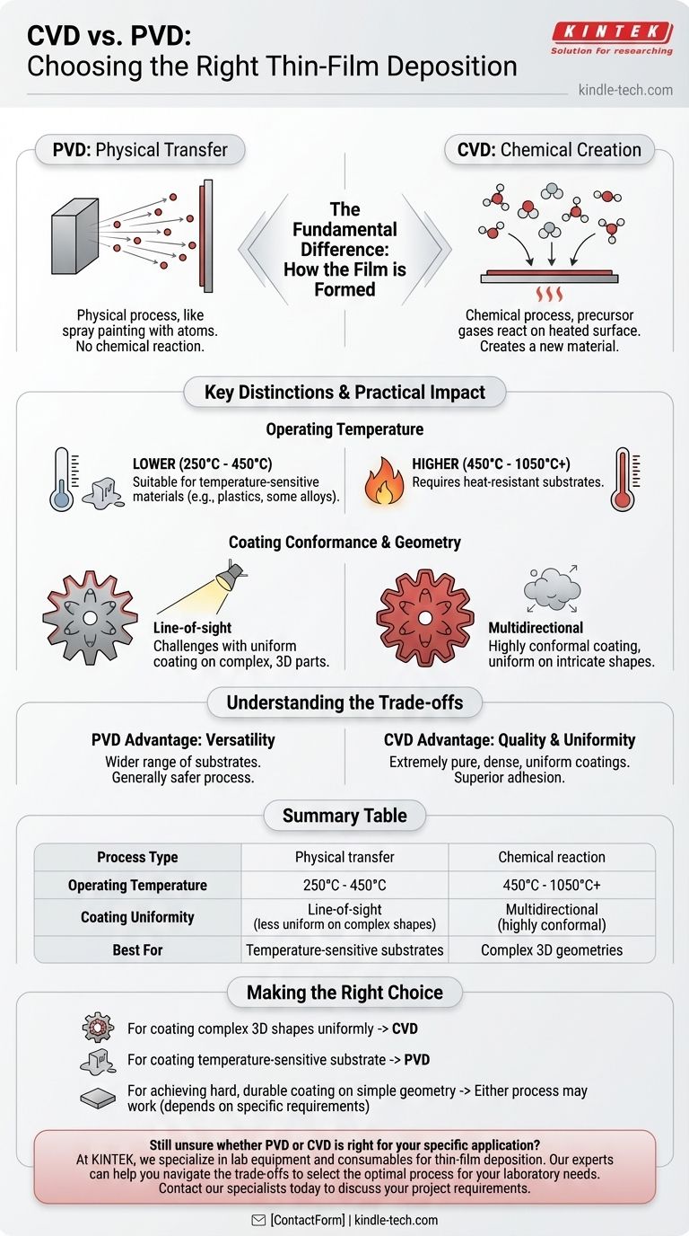
At its core, the distinction is straightforward. Physical Vapor Deposition (PVD) is a physical process that transfers a coating material from a solid source to a substrate, much like spray painting with atoms. In contrast, Chemical Vapor Deposition (CVD) is a chemical process where precursor gases react on a heated substrate surface to form a new, solid film.
The choice between PVD and CVD is not about which is "better," but which is appropriate. Your decision will be dictated by three primary factors: the temperature your substrate can withstand, the complexity of your part's geometry, and the specific film properties you require.
The Fundamental Difference: How the Film is Formed
The names themselves reveal the primary distinction. One process relies on physics, the other on chemistry. This fundamental difference dictates everything from operating temperature to the type of parts that can be successfully coated.
How PVD Works: A Physical Transfer
In PVD, a solid coating material is vaporized in a vacuum through methods like sputtering or thermal evaporation. This vapor then travels in a straight line and physically condenses onto the substrate, forming the thin film.
There is no chemical reaction involved on the surface of the part being coated. The deposited material is the same as the source material, just transferred from one location to another.
How CVD Works: A Chemical Creation
In CVD, various precursor gases are introduced into a reaction chamber containing a heated substrate. The high temperature provides the energy for these gases to react with each other and the substrate's surface.
This chemical reaction creates a new solid material directly on the surface, which becomes the coating. The resulting film is a compound formed from the constituent elements in the precursor gases.
Key Distinctions and Their Practical Impact
Understanding the core mechanism allows us to see how each process is better suited for different applications. The practical consequences of a physical versus a chemical process are significant.
Operating Temperature
PVD operates at lower temperatures, typically between 250°C and 450°C. This makes it suitable for coating materials that cannot withstand high heat, including some steels, alloys, and plastics.
CVD requires much higher temperatures, often ranging from 450°C to over 1050°C, to drive the necessary chemical reactions. This limits its use to substrates that can maintain their structural integrity at extreme heat.
Coating Conformance and Geometry
PVD is a line-of-sight process. Because the vaporized material travels in a straight line, it can only coat surfaces that are directly exposed to the source. This makes it challenging to achieve a uniform coating on complex, three-dimensional parts with internal surfaces or hidden features.
CVD is a multidirectional process. The precursor gases flow and surround the substrate, allowing the chemical reaction to occur on all exposed surfaces simultaneously. This results in a highly conformal coating that is uniform even on intricate shapes.
Understanding the Trade-offs
Neither technology is a universal solution. The advantages of one process are often linked to inherent limitations that you must consider for your specific goal.
The PVD Advantage: Versatility
PVD's main advantage is its lower operating temperature, which opens up a much wider range of substrate materials. The process is also generally considered safer as it does not always require the highly toxic or volatile precursor gases common in CVD.
However, the line-of-sight limitation is a significant trade-off. Achieving uniform coatings on complex parts often requires sophisticated rotating fixtures, which adds cost and complexity to the process.
The CVD Advantage: Quality and Uniformity
CVD's strength lies in its ability to produce extremely pure, dense, and uniform coatings on even the most complex shapes. The strong chemical bond formed between the film and the substrate often results in superior adhesion.
The primary trade-off is the high temperature, which immediately disqualifies many materials. Furthermore, managing the chemical precursors can add safety and handling complexities to the operation.
Making the Right Choice for Your Application
To select the correct technology, evaluate your project against the core strengths of each process.
- If your primary focus is coating complex 3D shapes uniformly: CVD is almost always the superior choice due to its conformal nature.
- If your primary focus is coating a temperature-sensitive substrate: PVD is the clear and necessary option because of its lower process temperatures.
- If your primary focus is achieving a hard, durable coating on a simple geometry: Either process may work, and the decision will depend on the specific material, adhesion requirements, and cost considerations.
By understanding how the underlying process dictates the outcome, you can make an informed decision that aligns with your engineering goals.
Summary Table:
| Feature | PVD (Physical Vapor Deposition) | CVD (Chemical Vapor Deposition) |
|---|---|---|
| Process Type | Physical transfer | Chemical reaction |
| Operating Temperature | 250°C - 450°C | 450°C - 1050°C+ |
| Coating Uniformity | Line-of-sight (less uniform on complex shapes) | Multidirectional (highly conformal) |
| Best For | Temperature-sensitive substrates | Complex 3D geometries |
Still unsure whether PVD or CVD is right for your specific application?
At KINTEK, we specialize in lab equipment and consumables for thin-film deposition. Our experts can help you navigate the trade-offs between temperature, geometry, and coating properties to select the optimal process for your laboratory needs.
Contact our specialists today to discuss your project requirements and discover how our solutions can enhance your research and development outcomes.
Visual Guide
Related Products
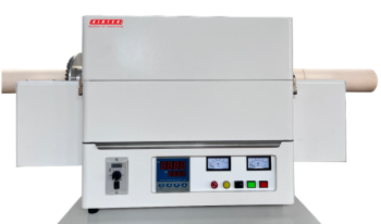
- Inclined Rotary Plasma Enhanced Chemical Vapor Deposition PECVD Equipment Tube Furnace Machine
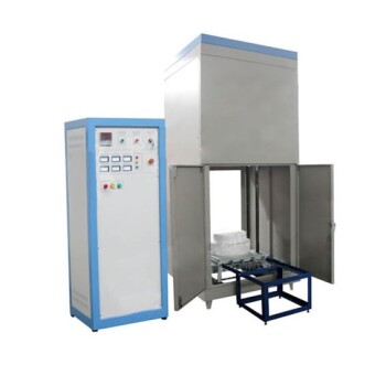
- Vacuum Hot Press Furnace Machine for Lamination and Heating
- HFCVD Machine System Equipment for Drawing Die Nano-Diamond Coating
- 915MHz MPCVD Diamond Machine Microwave Plasma Chemical Vapor Deposition System Reactor
- Laboratory Rapid Thermal Processing (RTP) Quartz Tube Furnace
People Also Ask
- How does plasma enhanced CVD work? Achieve Low-Temperature, High-Quality Thin Film Deposition
- What is the difference between PECVD and CVD? Unlock the Right Thin-Film Deposition Method
- What is the difference between CVD and PECVD? Choose the Right Thin-Film Deposition Method
- What is plasma in CVD process? Lowering Deposition Temperatures for Heat-Sensitive Materials
- What is meant by vapor deposition? A Guide to Atomic-Level Coating Technology