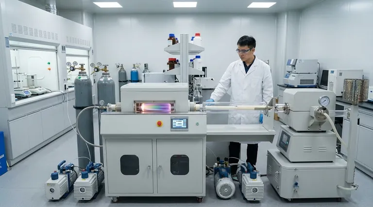
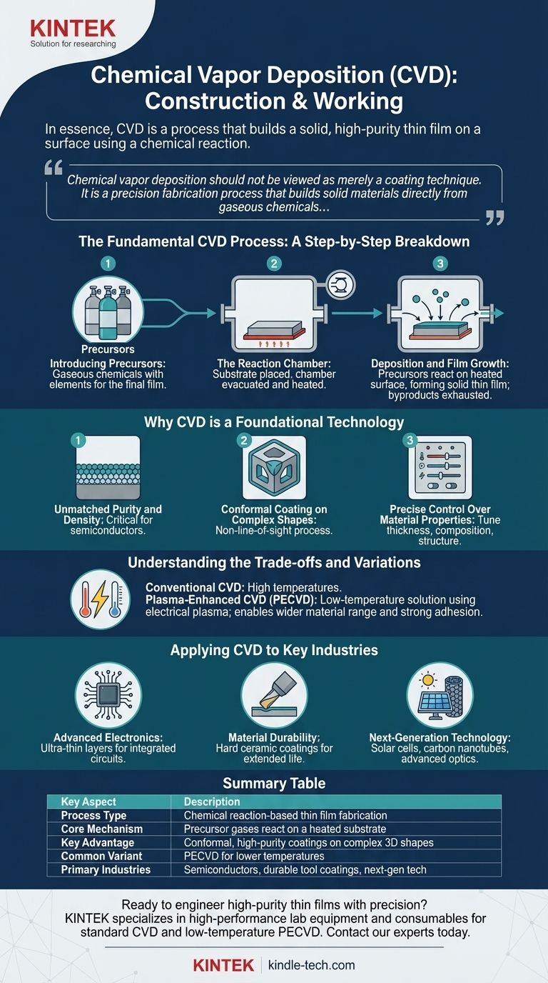
In essence, chemical vapor deposition (CVD) is a process that builds a solid, high-purity thin film on a surface using a chemical reaction rather than simple coating. A workpiece, or substrate, is placed in a reaction chamber where specific gases are introduced. These gases react on the heated surface of the substrate, decomposing to form the desired solid material layer-by-layer.
Chemical vapor deposition should not be viewed as merely a coating technique. It is a precision fabrication process that builds solid materials directly from gaseous chemicals, enabling the creation of exceptionally pure, uniform, and thin films on even the most complex surfaces.
The Fundamental CVD Process: A Step-by-Step Breakdown
To understand CVD, it's best to visualize it as a controlled, constructive process where a new material is grown directly onto a target object.
Step 1: Introducing the Precursors
The process begins by introducing carefully selected gaseous chemicals, known as precursors, into a reaction chamber. These gases contain the elements required for the final film (e.g., silicon-containing gases to create a silicon film).
Step 2: The Reaction Chamber
The target object, or substrate, is placed inside this sealed chamber. The chamber is typically under a vacuum and heated to a specific temperature required to drive the chemical reaction.
Step 3: Deposition and Film Growth
When the hot precursor gases come into contact with the heated substrate, a chemical reaction occurs directly on the surface. This reaction breaks the gases down, and the desired solid material deposits onto the substrate, forming a thin, solid film. Other chemical byproducts are simply exhausted from the chamber.
Why CVD is a Foundational Technology
CVD is not just one technique among many; its unique characteristics make it indispensable in high-performance applications.
Unmatched Purity and Density
Because the film is built from a chemical reaction using highly pure gases, the resulting layer is exceptionally pure and dense. This is critical for applications like semiconductors, where impurities can ruin device performance.
Conformal Coating on Complex Shapes
CVD is a non-line-of-sight process. The gas flows around the entire substrate, ensuring that even complex, three-dimensional shapes receive a perfectly uniform coating. This "wrap-around" capability is difficult to achieve with physical coating methods.
Precise Control Over Material Properties
By adjusting parameters like temperature, pressure, and gas composition, operators have fine-grained control over the final film. This allows for the tuning of its thickness, chemical composition, crystal structure, and grain size.
Understanding the Trade-offs and Variations
While powerful, the standard CVD process has inherent limitations that have led to important innovations.
The High-Temperature Requirement
Conventional CVD often requires very high temperatures to initiate the necessary chemical reactions. This can damage heat-sensitive substrates, such as certain plastics or electronic components that are already partially assembled.
Plasma-Enhanced CVD (PECVD): The Low-Temperature Solution
To overcome this limitation, Plasma-Enhanced CVD (PECVD) was developed. This method uses an electrical field to generate plasma, an energized state of gas. The plasma provides the energy for the chemical reaction, allowing deposition to occur at much lower temperatures.
PECVD enables the coating of a wider range of materials and produces dense films with strong adhesion, making it highly versatile.
Applying CVD to Key Industries
The unique capabilities of CVD make it a cornerstone process across several critical fields.
- If your primary focus is advanced electronics: CVD is essential for depositing the ultra-thin, high-purity layers of insulating, conducting, and semiconducting materials needed to manufacture integrated circuits.
- If your primary focus is material durability: CVD is used to apply hard, corrosion-resistant ceramic coatings (like titanium nitride) to cutting tools, extending their life and improving performance.
- If your primary focus is next-generation technology: The process is used to create thin-film solar cells, grow materials like carbon nanotubes, and develop advanced optical coatings.
Ultimately, chemical vapor deposition provides an unparalleled level of control for engineering materials from the atom up.
Summary Table:
| Key Aspect | Description |
|---|---|
| Process Type | Chemical reaction-based thin film fabrication |
| Core Mechanism | Precursor gases react on a heated substrate |
| Key Advantage | Conformal, high-purity coatings on complex 3D shapes |
| Common Variant | Plasma-Enhanced CVD (PECVD) for lower temperatures |
| Primary Industries | Semiconductors, durable tool coatings, next-gen tech |
Ready to engineer high-purity thin films with precision?
The controlled process of Chemical Vapor Deposition is critical for creating the advanced materials that power modern technology. Whether your lab requires standard CVD or low-temperature PECVD solutions for sensitive substrates, KINTEK specializes in providing the high-performance lab equipment and consumables you need to achieve exceptional results.
Contact our experts today to discuss how our CVD solutions can enhance your research and development in semiconductors, durable coatings, and next-generation materials.
Visual Guide
Related Products
- Chemical Vapor Deposition CVD Equipment System Chamber Slide PECVD Tube Furnace with Liquid Gasifier PECVD Machine
- RF PECVD System Radio Frequency Plasma-Enhanced Chemical Vapor Deposition RF PECVD
- Microwave Plasma Chemical Vapor Deposition MPCVD Machine System Reactor for Lab and Diamond Growth
- Customer Made Versatile CVD Tube Furnace Chemical Vapor Deposition Chamber System Equipment
- 915MHz MPCVD Diamond Machine Microwave Plasma Chemical Vapor Deposition System Reactor
People Also Ask
- What is the chemical vapor deposition growth process? Build Superior Thin Films from the Atom Up
- What types of substrates are used in CVD to facilitate graphene films? Optimize Graphene Growth with the Right Catalyst
- What are the processes of vapor phase deposition? Understand CVD vs. PVD for Superior Thin Films
- Why is Chemical Vapor Deposition (CVD) equipment uniquely suited for constructing hierarchical superhydrophobic structures?
- What are the advantages of chemical vapor deposition? Achieve Superior Thin Films for Your Lab


