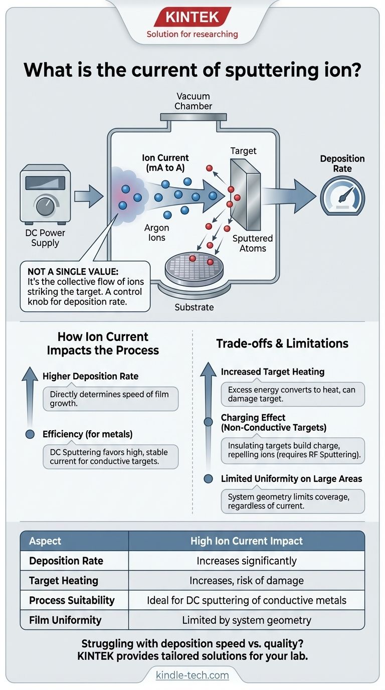
To be precise, there is no single value for the "current of a sputtering ion." This term refers to the overall ion current—the collective flow of charged ions striking the target material—which is a critical and highly variable process parameter. This current is controlled by the power supply and directly determines the rate at which material is deposited onto your substrate.
The central concept to grasp is that ion current is not a fixed property, but a control knob for the sputtering process. Increasing the ion current directly increases the number of ions hitting the target per second, which speeds up the deposition rate but also introduces crucial trade-offs related to heat and film quality.
What "Ion Current" Means in Sputtering
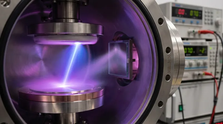
In any sputtering system, the goal is to use high-energy ions (typically of an inert gas like Argon) as microscopic projectiles to chip atoms away from a source material, known as the "target." The "ion current" is the measure of how many of these projectiles are hitting the target over a period of time.
From a Single Ion to a Measurable Current
A single ion carries a fundamental electric charge. However, the current we measure and control in a sputtering system is the macroscopic flow of billions of these ions. This is typically measured in milliamps (mA) or amps (A) and is regulated by the system's power supply.
The Role of the Power Supply
The power supply, such as the Direct Current (DC) source used in DC sputtering, creates a strong electric field. This field accelerates the positively charged gas ions toward the negatively charged target, creating a steady and controllable ion current.
Ion Current as Your Primary Control Knob
Think of the ion current as the primary dial for deposition speed. A higher current means more ions are bombarding the target each second. This dislodges more target atoms, resulting in a faster-growing film on your substrate.
How Ion Current Impacts the Sputtering Process
Controlling the ion current is fundamental because it directly influences the speed, efficiency, and final characteristics of your thin film.
The Direct Link to Deposition Rate
The most immediate effect of increasing ion current is a higher deposition rate. For processes involving large-scale coating of pure metals, techniques like DC sputtering are favored precisely because they can efficiently sustain a high, stable ion current.
The Distinction from Ion Energy
It is critical to distinguish ion current from ion energy. While current dictates the quantity of sputtering ions, energy dictates their impact force. Ion beam sputtering, for example, is noted for its high particle energy (around 10 eV), which is roughly 100 times that of vacuum evaporation. This high energy ensures sputtered atoms embed firmly into the substrate, creating exceptionally strong bonds and high-quality films.
The Case of DC Sputtering
DC sputtering is a perfect illustration of using current effectively. It applies a constant DC voltage to a target, creating a continuous flow of ions. This method is highly effective and cost-efficient for targets that are electrically conductive, like pure metals, as the current can flow without interruption.
Understanding the Trade-offs and Limitations
While increasing ion current sounds like a simple way to speed up work, it comes with significant consequences that must be managed.
The Problem of Target Heating
A higher ion current means more energy is being transferred to the target. A significant portion of this energy is converted into heat. Excessive heating can damage the target, alter its sputtering characteristics, or even cause the film's properties to drift during deposition.
The Challenge of Non-Conductive Targets
You cannot use a simple DC power source for electrically insulating (dielectric) targets. As positive ions strike the insulating target, a positive charge builds up on its surface. This "charging" effect quickly repels incoming ions, choking off the ion current and stopping the sputtering process. This is why other techniques, like RF (Radio Frequency) sputtering, are required for materials like oxides and nitrides.
Rate vs. Uniformity on Large Areas
Even with a high deposition rate driven by a strong ion current, some methods are not suitable for all applications. As noted with ion beam sputtering, the target area can be limited. This makes it difficult to achieve a uniform film thickness across a very large substrate, regardless of how high you set the current.
Matching the Process to Your Goal
The optimal ion current is entirely dependent on your material, system, and desired outcome.
- If your primary focus is high-speed, cost-effective coating of a pure metal: DC sputtering is likely the best approach, as it is designed to sustain a high, stable ion current for conductive targets.
- If your primary focus is achieving the highest possible film quality and adhesion: Ion beam sputtering is a superior choice, as the process prioritizes high ion energy to create dense, strongly bonded films.
- If your primary focus is coating a large surface with perfect uniformity: You must consider the system's geometry, as a high ion current alone will not solve the challenge of a limited target area.
Ultimately, mastering ion current is about balancing the need for speed against the constraints of your material and the quality requirements of your final product.
Summary Table:
| Aspect | High Ion Current Impact |
|---|---|
| Deposition Rate | Increases significantly |
| Target Heating | Increases, risk of damage |
| Process Suitability | Ideal for DC sputtering of conductive metals |
| Film Uniformity (Large Areas) | Limited by system geometry, not just current |
Struggling to balance deposition speed with film quality in your lab?
At KINTEK, we specialize in lab equipment and consumables for precise thin-film deposition. Our experts can help you select the right sputtering system—whether you need the high-speed efficiency of DC sputtering for metals or the superior film quality of ion beam sputtering.
Let KINTEK provide the solution tailored to your laboratory's needs. Contact our experts today for a consultation on optimizing your sputtering process.
Visual Guide
Related Products
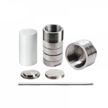
- High Pressure Laboratory Autoclave Reactor for Hydrothermal Synthesis
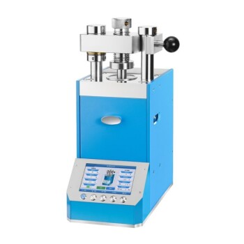
- Metallographic Specimen Mounting Machine for Laboratory Materials and Analysis
- Automatic Lab Cold Isostatic Press CIP Machine Cold Isostatic Pressing
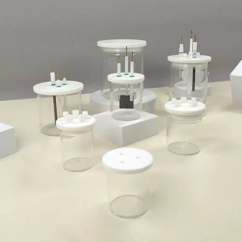
- Quartz Electrolytic Electrochemical Cell for Electrochemical Experiments
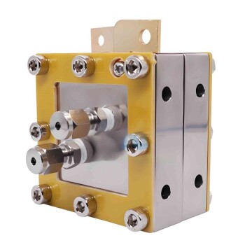
- Customizable PEM Electrolysis Cells for Diverse Research Applications
People Also Ask
- What is the pressure in a batch reactor? A Guide to Dynamic Control and Safety
- Which solvent is normally used in IR spectroscopy? Optimize Your Sample Prep for Clearer Results
- What is a high pressure high temperature autoclave reactor? Unlock Extreme Chemical Synthesis
- Does pressure affect melting and boiling? Master Phase Changes with Pressure Control
- What are the analytical used in laboratory? Choose the Right Tool for Your Lab's Needs