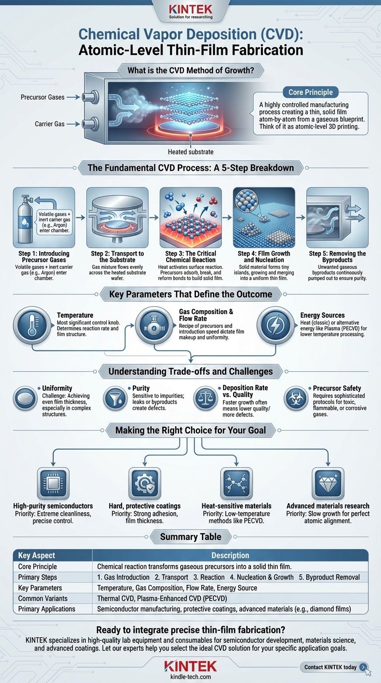
At its core, Chemical Vapor Deposition (CVD) is a highly controlled manufacturing process used to create a thin, solid film on top of a surface, known as a substrate. It works by introducing specific gases, called precursors, into a chamber. A chemical reaction, typically activated by heat, causes these gases to decompose and deposit a layer of material atom-by-atom onto the substrate, building the desired film.
The true power of CVD lies in its ability to construct materials from the ground up. Think of it not as simple coating, but as atomic-level 3D printing where a gaseous blueprint is precisely transformed into a solid structure on a target surface.
The Fundamental CVD Process: A Step-by-Step Breakdown
To understand CVD, it's best to visualize it as a sequence of five distinct events occurring within a controlled reaction chamber.
Step 1: Introducing Precursor Gases
The process begins by feeding one or more volatile precursor gases into the reaction chamber. These gases contain the atoms required for the final film (e.g., gases containing silicon for a silicon film).
Often, these precursors are diluted with an inert carrier gas (like argon or nitrogen) that helps transport them through the system at a controlled rate.
Step 2: Transport to the Substrate
This mixture of gases flows through the chamber and across the surface of the substrate wafer. The engineering of the chamber and the gas flow dynamics are critical for ensuring every part of the substrate is exposed to the gases evenly.
Step 3: The Critical Chemical Reaction
The substrate is heated to a precise, high temperature (often several hundred degrees Celsius). When the cooler precursor gases make contact with this hot surface, they gain the energy needed to react.
This is a surface-catalyzed reaction. The gases adsorb, or stick, to the substrate surface, which provides the perfect site for the chemical bonds to break and reform, creating the solid material for the film.
Step 4: Film Growth and Nucleation
The deposition doesn't happen all at once. The solid material begins to form as tiny, isolated islands on the substrate.
As the process continues, these islands grow larger and eventually merge, forming a continuous, uniform thin film across the entire surface.
Step 5: Removing the Byproducts
The chemical reactions that form the solid film also produce unwanted gaseous byproducts. These waste gases are continuously pumped out of the chamber, ensuring they do not interfere with the film's purity or growth.
Key Parameters That Define the Outcome
The final properties of the film—its thickness, composition, and quality—are dictated by several critical process parameters.
The Role of Temperature
Substrate temperature is the most significant control knob. It determines the rate of the chemical reaction and can influence the final film's crystalline structure. Too low, and the reaction won't occur; too high, and you might get unwanted side reactions.
Gas Composition and Flow Rate
The "recipe" of precursor gases dictates the film's chemical makeup. The rate at which they are introduced affects the growth speed and can impact the film's uniformity.
Energy Sources Beyond Heat
While a heated substrate is the classic method, some materials or substrates are sensitive to high temperatures. In these cases, other energy sources can be used to drive the reaction.
A common variant is Plasma-Enhanced CVD (PECVD), where an RF plasma field energizes the gases, allowing deposition to occur at much lower temperatures. Other methods use lasers or hot filaments to supply the necessary energy.
Understanding the Trade-offs and Challenges
While powerful, CVD is a complex process with inherent engineering challenges that must be managed.
Uniformity and Coverage
Achieving a perfectly uniform film thickness across a large wafer, or inside complex, three-dimensional trenches, is a significant challenge. It requires precise control over gas flow and temperature distribution.
Purity and Contamination
The process is extremely sensitive to impurities. Any unwanted molecules in the chamber—from a small leak or from byproducts—can become trapped in the film, creating defects that degrade its performance. For example, during diamond growth, technicians must periodically halt the process to clean away unwanted graphite.
Deposition Rate vs. Quality
There is often a direct trade-off between speed and perfection. Growing a film faster can save time and money, but it often leads to a less ordered, lower-quality structure with more defects. High-purity applications, like in semiconductors, demand slow, careful growth.
Precursor Safety
The gases used in CVD can be highly toxic, flammable, or corrosive. This necessitates sophisticated safety and handling protocols, adding to the complexity and cost of the operation.
Making the Right Choice for Your Goal
The specific CVD technique and parameters you choose depend entirely on the desired outcome for the final product.
- If your primary focus is high-purity semiconductor manufacturing: Your priority is extreme cleanliness and precise control over temperature and gas flow to create flawless crystalline layers.
- If your primary focus is creating hard, protective coatings on tools: You will likely use higher-temperature methods that prioritize strong adhesion and film thickness over perfect crystal structure.
- If your primary focus is depositing on heat-sensitive materials like polymers: You must use a low-temperature variant like Plasma-Enhanced CVD (PECVD) to avoid damaging the substrate.
- If your primary focus is advanced materials research, like lab-grown diamonds: You are carefully balancing a slow growth rate for perfect atomic alignment against the practical constraints of production time.
Ultimately, mastering CVD is about a deep understanding of the interplay between chemistry, temperature, and pressure to build functional materials from a gaseous state.
Summary Table:
| Key Aspect | Description |
|---|---|
| Core Principle | A chemical reaction transforms gaseous precursors into a solid thin film on a substrate surface. |
| Primary Steps | 1. Gas Introduction 2. Transport 3. Reaction 4. Nucleation & Growth 5. Byproduct Removal |
| Key Parameters | Temperature, Gas Composition, Flow Rate, Energy Source (e.g., Heat, Plasma) |
| Common Variants | Thermal CVD, Plasma-Enhanced CVD (PECVD) |
| Primary Applications | Semiconductor manufacturing, protective coatings, advanced materials (e.g., diamond films) |
Ready to integrate precise thin-film fabrication into your research or production? The right lab equipment is critical for controlling the complex parameters of Chemical Vapor Deposition. KINTEK specializes in high-quality lab equipment and consumables, serving the precise needs of laboratories in semiconductor development, materials science, and advanced coatings. Let our experts help you select the ideal CVD solution for your specific application goals. Contact KINTEK today to discuss your project requirements!
Visual Guide
Related Products
- CVD Diamond Dressing Tools for Precision Applications
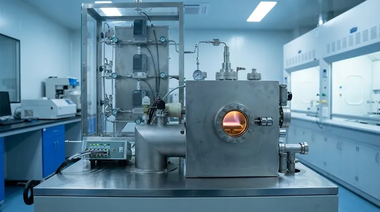
- Multi Heating Zones CVD Tube Furnace Machine Chemical Vapor Deposition Chamber System Equipment
- CVD Diamond Domes for Industrial and Scientific Applications
- CVD Diamond for Thermal Management Applications
- Chemical Vapor Deposition CVD Equipment System Chamber Slide PECVD Tube Furnace with Liquid Gasifier PECVD Machine
People Also Ask
- What color diamonds are CVD? Understanding the Process from Brown Tint to Colorless Beauty
- How long does it take to make synthetic diamonds? Discover the 6-8 Week Science Behind Lab-Grown Gems
- What is chemical vapor deposition of diamond? Grow High-Purity Diamonds Atom-by-Atom
- What are the disadvantages of CVD diamonds? Understanding the trade-offs for your purchase.
- How do you identify a CVD diamond? The Definitive Guide to Lab-Grown Diamond Verification


