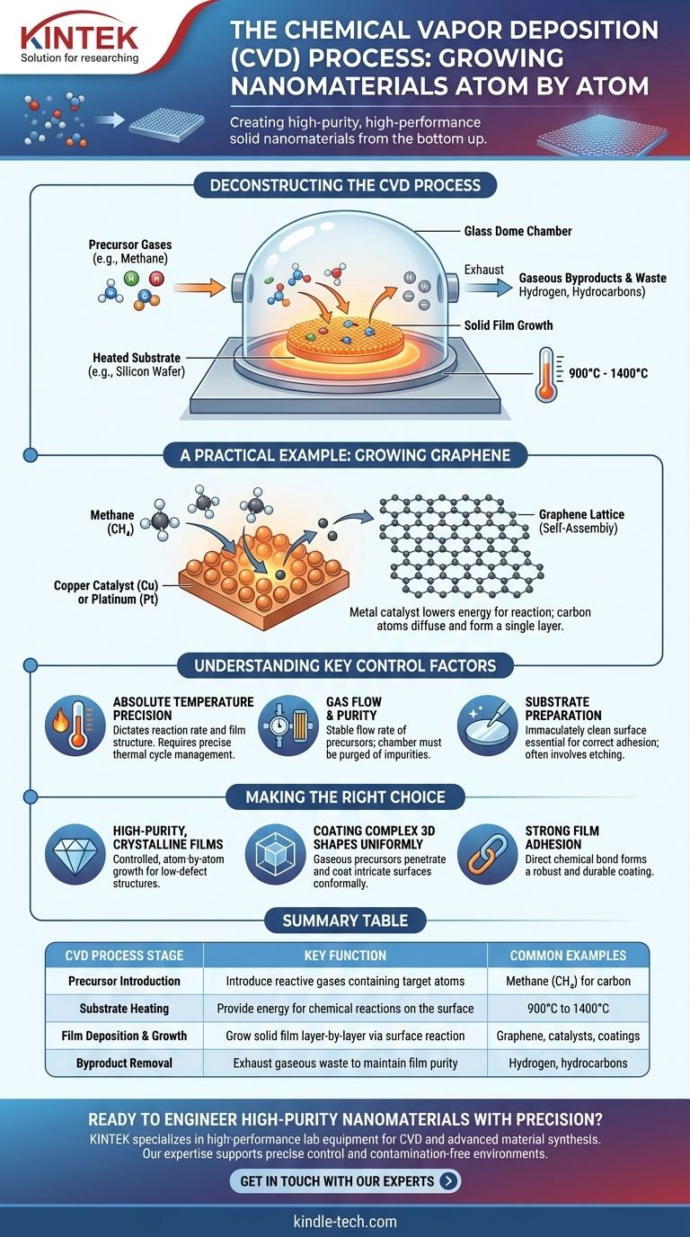
At its core, Chemical Vapor Deposition (CVD) is a sophisticated manufacturing process used to create high-purity, high-performance solid nanomaterials from the bottom up. It involves introducing reactive precursor gases into a chamber where they undergo a chemical reaction on a heated surface, or substrate, to form an ultra-thin, solid film. This technique is fundamental to producing materials like graphene, catalysts, and advanced coatings.
The central concept of CVD is not merely coating a surface, but rather growing a new material layer directly onto it. It transforms gaseous building blocks into a solid, highly-ordered film through controlled chemical reactions in a high-temperature environment.
Deconstructing the CVD Process: From Gas to Solid Film
To truly understand CVD, we must look at its core components and the sequence of events that enables atomic-level construction. The entire process is a carefully orchestrated balance of chemistry, temperature, and pressure.
The Reaction Chamber and Substrate
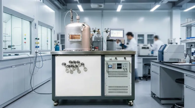
The process begins inside a sealed reaction chamber, which provides a highly controlled environment. Inside, one or more substrates—the materials to be coated, such as a silicon wafer or a copper foil—are placed. The substrate serves as the foundation for the new material growth.
The Precursor Gases
One or more volatile precursor gases are introduced into the chamber. These gases contain the specific atoms required for the final film. For example, to grow graphene (a form of carbon), a carbon-bearing gas like methane is used.
The Role of Extreme Heat
The substrate is typically heated to extremely high temperatures, often between 900°C and 1400°C. This intense heat is not just for warming; it provides the necessary energy to break the chemical bonds in the precursor gases, making them highly reactive.
Deposition and Film Growth
As the reactive gas molecules come into contact with the hot substrate, a chemical reaction occurs exclusively on its surface. The solid product of this reaction deposits onto the substrate, forming a thin film. This film grows layer by layer, resulting in a crystalline or amorphous structure depending on the process parameters.
Removal of Byproducts
The chemical reaction also produces gaseous byproducts, which are effectively waste. These are continuously removed from the chamber through an exhaust system, ensuring the purity of the growing film.
A Practical Example: Growing Graphene
The synthesis of graphene is a perfect illustration of the CVD process in action. It highlights how the substrate can play a more active role than just being a passive surface.
The Metal Catalyst Substrate
For graphene growth, a metallic substrate like copper (Cu) or platinum (Pt) is used. This metal is not just the foundation but also acts as a catalyst. It dramatically lowers the energy required to break down the carbon-bearing precursor gas.
The Carbon Source
A gas like methane (CH₄) is introduced into the chamber. At high temperatures, the copper catalyst helps decompose the methane, freeing the carbon atoms.
Self-Assembling into Graphene
These newly freed carbon atoms diffuse and arrange themselves on the copper surface, forming the characteristic hexagonal lattice of a single layer of graphene. Once the process is complete, this atomic-scale sheet of graphene can be carefully separated from the metal and transferred to a different, more practical substrate like silicon.
Understanding the Key Control Factors
The quality of the nanomaterial produced via CVD is entirely dependent on precise control over several key variables. Any deviation can compromise the final product's integrity.
Absolute Temperature Precision
Temperature control is the most critical factor. It dictates the rate of the chemical reaction and the final structure of the film. The entire thermal cycle—heating, deposition, and cooling—must be managed precisely to prevent defects.
Gas Flow and Purity
The flow rate of precursor and carrier gases into the chamber must be stable. Furthermore, the chamber must be purged of any residual oxygen or moisture, as these impurities can cause unwanted side reactions and contaminate the film.
Substrate Preparation
The substrate surface must be immaculately clean and properly prepared before deposition. This often involves a process called etching to remove any passivation layers or contaminants that would prevent the film from adhering correctly.
Making the Right Choice for Your Goal
CVD is an exceptionally powerful and versatile technique, but its suitability depends entirely on your specific material and application requirements.
- If your primary focus is high-purity, crystalline films: CVD is ideal because the slow, controlled, atom-by-atom growth process allows for the formation of highly-ordered, low-defect structures.
- If your primary focus is coating complex 3D shapes uniformly: The gaseous nature of the precursors allows them to penetrate and coat intricate surfaces conformally, something that line-of-sight methods cannot achieve.
- If your primary focus is strong film adhesion to a substrate: The process forms a direct chemical bond between the film and the substrate, resulting in a much more robust and durable coating than purely physical methods.
Ultimately, mastering the CVD process is about mastering the control of a chemical reaction at a material's surface to engineer new materials with unmatched precision.
Summary Table:
| CVD Process Stage | Key Function | Common Examples |
|---|---|---|
| Precursor Introduction | Introduce reactive gases containing target atoms | Methane (CH₄) for carbon |
| Substrate Heating | Provide energy for chemical reactions on the surface | 900°C to 1400°C |
| Film Deposition & Growth | Grow solid film layer-by-layer via surface reaction | Graphene, catalysts, coatings |
| Byproduct Removal | Exhaust gaseous waste to maintain film purity | Hydrogen, hydrocarbons |
Ready to engineer high-purity nanomaterials with precision?
The CVD process is fundamental for creating advanced materials like graphene, catalysts, and durable coatings. At KINTEK, we specialize in providing the high-performance lab equipment and consumables you need to master chemical vapor deposition and other advanced material synthesis techniques.
Our expertise supports your laboratory in achieving precise temperature control, stable gas flow, and contamination-free environments—critical factors for successful CVD outcomes.
Contact us today to discuss your specific application and discover how KINTEK can enhance your nanomaterial research and production.
Get in touch with our experts →
Visual Guide
Related Products
- Customer Made Versatile CVD Tube Furnace Chemical Vapor Deposition Chamber System Equipment
- Chemical Vapor Deposition CVD Equipment System Chamber Slide PECVD Tube Furnace with Liquid Gasifier PECVD Machine
- CVD Diamond for Thermal Management Applications
- Custom CVD Diamond Coating for Lab Applications
- HFCVD Machine System Equipment for Drawing Die Nano-Diamond Coating
People Also Ask
- What is the synthesis and mechanism involved in the preparation of carbon nanotubes using CVD process? Master Controlled Growth for Your Application
- What is the application of CVD in nanotechnology? Harness Atomic-Level Precision for Next-Gen Materials
- What is a CVD tube furnace? A Complete Guide to Thin-Film Deposition
- What is the difference between hot wall CVD and cold wall CVD? Choose the Right System for Your Process
- What is the meaning of synthesis of graphene? A Guide to Top-Down vs. Bottom-Up Methods


