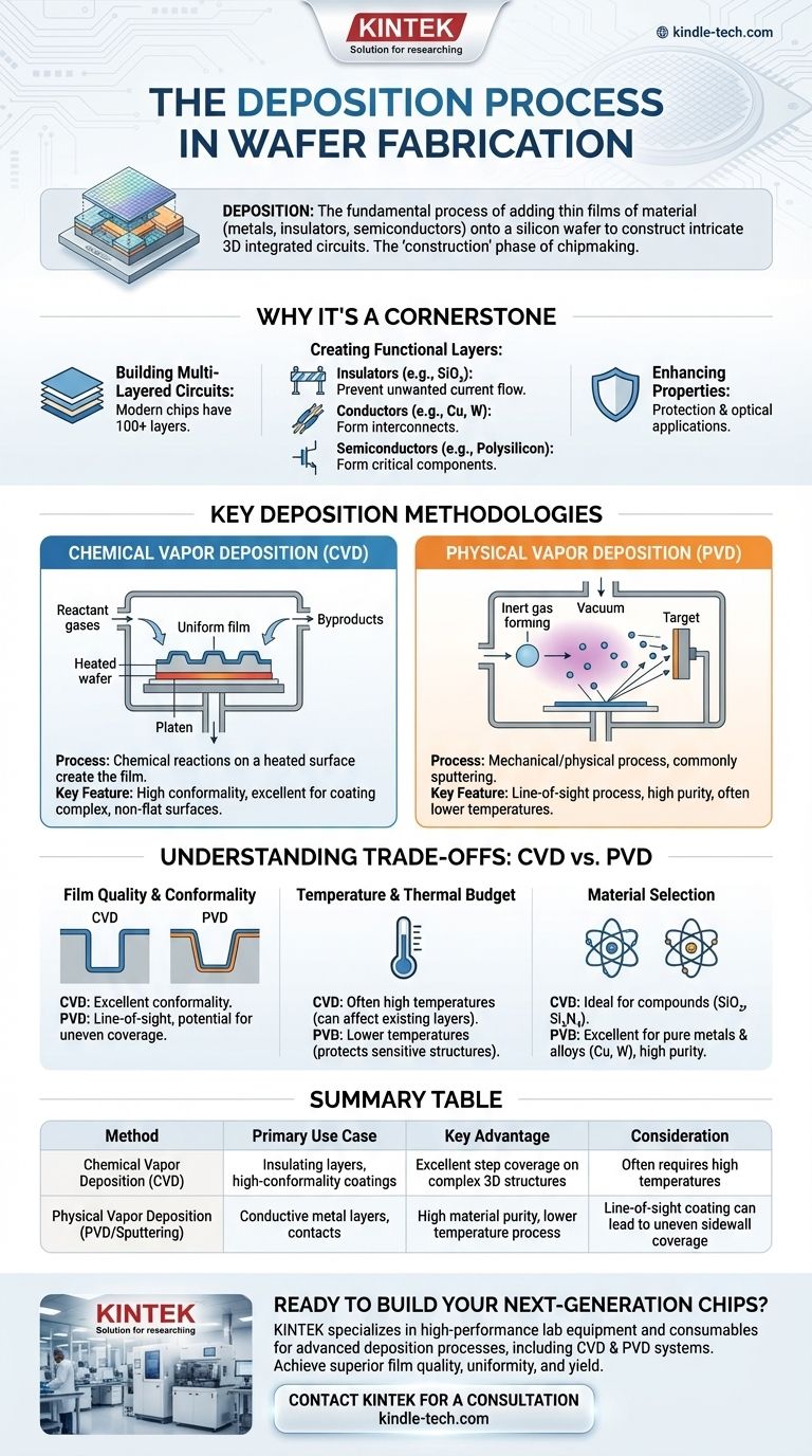
In wafer fabrication, deposition is the fundamental process of adding a thin film of material onto a silicon wafer's surface. These layers, which can be metals, insulators, or semiconductors, are the essential building blocks used to construct the intricate, three-dimensional structures of integrated circuits, such as transistors and their interconnecting wiring.
The core of semiconductor manufacturing is a cycle of adding and removing materials to build a microscopic city on a silicon wafer. Deposition is the "construction" phase—the precise application of each new layer that will eventually become a functional part of the chip.
Why Deposition is a Cornerstone of Chipmaking
Deposition is not merely about adding a coating; it is a highly controlled engineering process designed to create layers with specific, predictable properties. Each deposited film serves a distinct purpose in the final device.
The Goal: Building a Multi-Layered Circuit
Modern microchips are not flat. They are incredibly complex 3D structures, often with over 100 distinct layers stacked on top of one another. Deposition is the process used to build each of these layers, one at a time.
Creating Conductive and Insulating Layers
The primary function of these films is to control the flow of electricity.
- Insulators, such as silicon dioxide, are deposited to prevent electrical current from flowing where it shouldn't.
- Conductors, such as copper or tungsten, are deposited to form the "wires" that connect the millions or billions of transistors on a chip.
- Semiconductors, like polysilicon, are deposited to form critical components of the transistors themselves, such as the gate.
Enhancing Substrate Properties
Beyond conductivity, deposited films can protect underlying layers from chemical or physical damage during subsequent manufacturing steps, or they can be specifically designed to interact with light in a certain way for optical applications.
Key Deposition Methodologies
While the goal is always to add a film, the method used depends heavily on the material being deposited and the required characteristics of the film, such as its purity and uniformity. The two dominant techniques are Chemical Vapor Deposition and Physical Vapor Deposition.
Chemical Vapor Deposition (CVD)
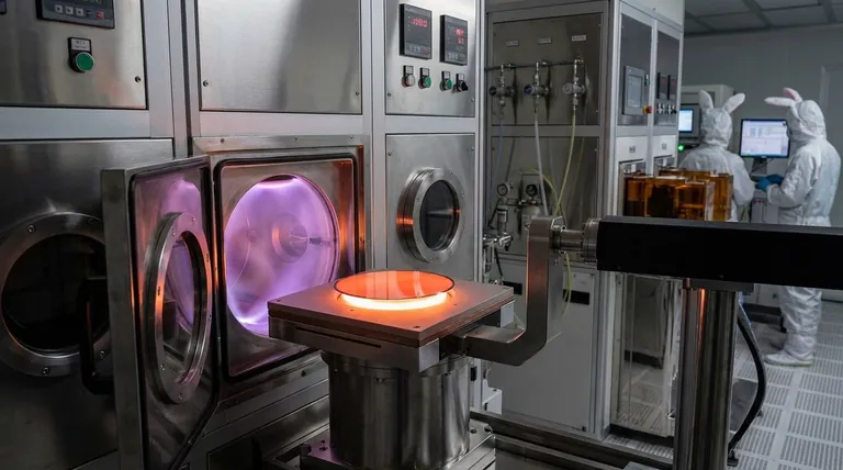
CVD is a process that uses chemical reactions to create the film. Reactant gases are introduced into a chamber containing the wafer. These gases adsorb onto the hot wafer surface, react to form a solid film, and then release gaseous byproducts that are removed from the chamber.
This process is excellent for creating highly uniform films that can conform perfectly to complex, non-flat surfaces on the wafer—a property known as high conformality.
Physical Vapor Deposition (PVD)
PVD, in contrast, is a mechanical or physical process. The most common form is sputtering.
- A chamber is put under a high vacuum to remove contaminants.
- An inert gas, such as argon, is introduced to create a plasma.
- This plasma is used to bombard a "target" made of the material to be deposited.
- The bombardment physically knocks atoms off the target, which then travel and coat the wafer, forming a thin film.
PVD is often described as a "line-of-sight" process, similar to spray painting, as the sputtered atoms travel in a relatively straight line from the target to the wafer.
Understanding the Trade-offs: CVD vs. PVD
Choosing between CVD and PVD involves critical trade-offs related to the specific layer being built. There is no single "best" method; the choice is dictated by the engineering requirements of that particular step.
Film Quality and Conformality
CVD excels at coating intricate topographies because the reactant gases can diffuse into and react within deep trenches and complex shapes. PVD's line-of-sight nature can result in thinner coatings on the sidewalls of a trench and thicker coatings at the top, which can be problematic.
Temperature and Thermal Budget
CVD processes often require high temperatures to drive the necessary chemical reactions. This can be a significant constraint, as the heat can potentially damage or alter layers that have already been fabricated on the wafer. Many PVD processes can operate at much lower temperatures, protecting the integrity of existing structures.
Material Selection
The material being deposited is a primary factor. CVD is ideal for compound materials like silicon dioxide (SiO₂) or silicon nitride (Si₃N₄). PVD, especially sputtering, is highly effective for depositing pure metals and alloys, offering excellent control over film purity.
How to Apply This to Your Goal
The selection of a deposition technique is a strategic decision based on the specific requirements of the film layer you are creating.
- If your primary focus is creating a uniform, insulating layer over complex topography: CVD is often the superior choice due to its excellent conformality, ensuring even coverage everywhere.
- If your primary focus is depositing a pure metal film for wiring or contacts: PVD/sputtering provides high purity and precise control in a process that is often more compatible with temperature-sensitive device structures.
- If your primary focus is managing the thermal budget to protect pre-existing layers: The lower-temperature nature of PVD may be a critical advantage over a high-temperature CVD process.
Ultimately, deposition is a versatile and indispensable tool, allowing chipmakers to precisely build the foundational layers that power all modern electronics.
Summary Table:
| Deposition Method | Primary Use Case | Key Advantage | Consideration |
|---|---|---|---|
| Chemical Vapor Deposition (CVD) | Insulating layers (e.g., SiO₂), high-conformality coatings | Excellent step coverage on complex 3D structures | Often requires high temperatures |
| Physical Vapor Deposition (PVD/Sputtering) | Conductive metal layers (e.g., Cu, W), contacts | High material purity, lower temperature process | Line-of-sight coating can lead to uneven sidewall coverage |
Ready to Build Your Next-Generation Chips?
The precise application of thin films is critical to your semiconductor fabrication success. KINTEK specializes in providing high-performance lab equipment and consumables for advanced deposition processes, including CVD and PVD systems.
We help our laboratory partners achieve superior film quality, uniformity, and yield. Contact us today to discuss how our solutions can meet your specific wafer fabrication needs.
Contact KINTEK for a Consultation
Visual Guide
Related Products
- Chemical Vapor Deposition CVD Equipment System Chamber Slide PECVD Tube Furnace with Liquid Gasifier PECVD Machine
- 915MHz MPCVD Diamond Machine Microwave Plasma Chemical Vapor Deposition System Reactor
- Split Chamber CVD Tube Furnace with Vacuum Station Chemical Vapor Deposition System Equipment Machine
- Customer Made Versatile CVD Tube Furnace Chemical Vapor Deposition Chamber System Equipment
- RF PECVD System Radio Frequency Plasma-Enhanced Chemical Vapor Deposition RF PECVD
People Also Ask
- What types of substrates are used in CVD to facilitate graphene films? Optimize Graphene Growth with the Right Catalyst
- What is plasma enhanced chemical vapor deposition PECVD equipment? A Guide to Low-Temperature Thin Film Deposition
- What are the processes of vapor phase deposition? Understand CVD vs. PVD for Superior Thin Films
- What are the core advantages of PE-CVD in OLED encapsulation? Protect Sensitive Layers with Low-Temp Film Deposition
- What are the advantages of chemical vapor deposition? Achieve Superior Thin Films for Your Lab


