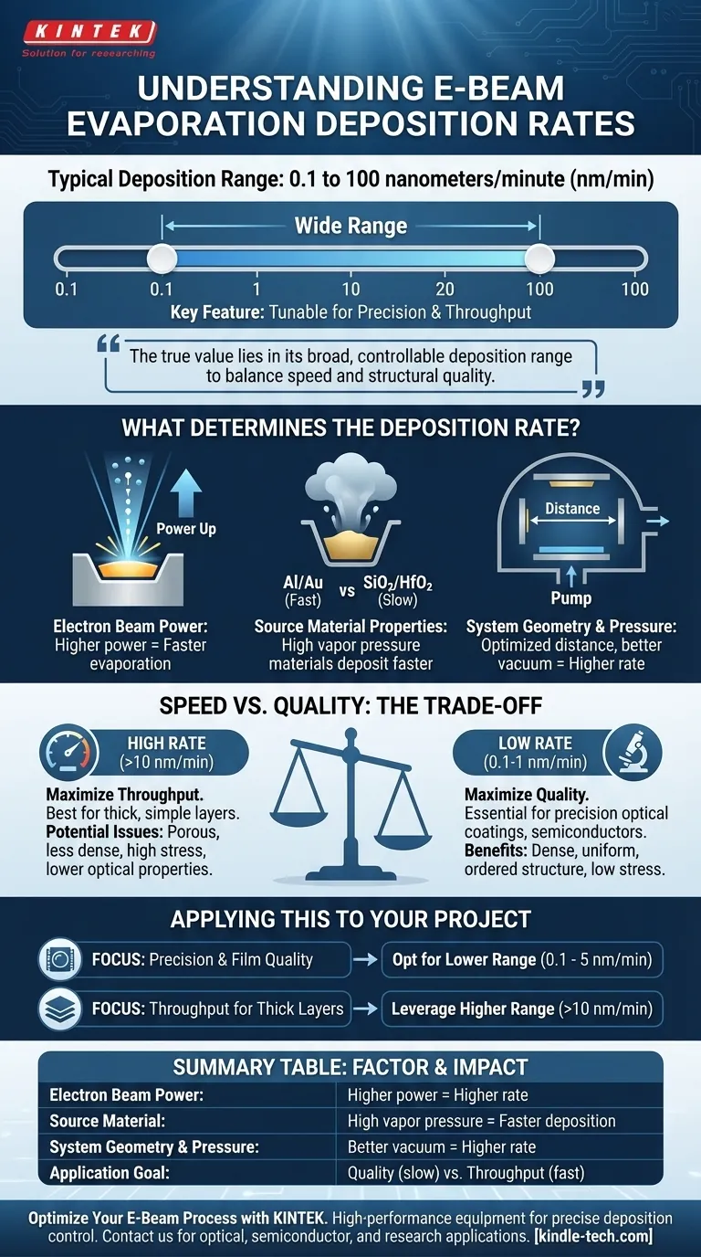
The typical deposition rate for e-beam evaporation ranges from 0.1 to 100 nanometers per minute (nm/min). This wide range is a key feature of the technology, allowing it to be adapted for both high-precision and high-throughput applications by carefully controlling the process parameters.
While often cited for its high-speed capabilities, the true value of e-beam evaporation lies in its broad and highly controllable deposition range. This allows you to precisely balance deposition speed against the required structural quality of the final thin film.
What Determines the Deposition Rate?
The rate at which material is deposited is not a fixed number. It is a dynamic variable influenced by several critical factors, giving you significant control over the film growth process.
Electron Beam Power
The most direct control you have is beam power. A higher power setting delivers more energy to the source material, increasing its temperature and causing it to evaporate more quickly. This directly translates to a higher deposition rate.
Source Material Properties
Every material behaves differently. Materials with a high vapor pressure at a given temperature, like aluminum or gold, will evaporate and deposit much faster than refractory materials like silicon dioxide (SiO₂) or hafnium dioxide (HfO₂) which require more energy to evaporate.
System Geometry and Pressure
The physical layout of the vacuum chamber plays a significant role. The distance and angle between the evaporation source and the substrate affect how many evaporated atoms successfully reach their target, influencing the net deposition rate. Lower chamber pressures (better vacuum) also improve efficiency by reducing collisions with background gas molecules.
Understanding the Trade-offs: Speed vs. Quality
Choosing a deposition rate is a fundamental compromise between manufacturing speed and the final quality of the thin film. There is no single "best" rate; it depends entirely on the application's requirements.
The Impact of High Deposition Rates
Pushing for a high rate (e.g., >10 nm/min) is ideal for maximizing throughput. This is common for applying thick, simple metallic or protective layers where microscopic structure is less critical.
However, rapid deposition can lead to a more porous, less dense film structure and higher internal stress. This can negatively impact optical properties, adhesion, and long-term stability.
The Value of Low Deposition Rates
A slow, controlled rate (e.g., 0.1 to 1 nm/min) is essential for creating high-quality, dense films. This deliberate pace allows atoms more time to settle into an ordered, stable structure on the substrate surface.
This level of control is non-negotiable for applications like precision optical coatings, semiconductors, and other electronic devices where film density, purity, and uniformity are paramount.
How to Apply This to Your Project
Your choice of deposition rate should be driven by the end goal for your thin film. The process must be tailored to the required performance characteristics.
- If your primary focus is precision and film quality: Opt for the lower end of the deposition range (0.1 - 5 nm/min) to ensure a dense, uniform, and low-stress film structure, which is critical for optical and electronic applications.
- If your primary focus is throughput for thick layers: You can leverage the higher end of the deposition range (>10 nm/min), provided the resulting film structure meets the mechanical or basic conductive requirements of your application.
Ultimately, the key advantage of e-beam evaporation is its tunability, allowing you to optimize the process for your specific balance of film quality and manufacturing speed.
Summary Table:
| Factor | Impact on Deposition Rate |
|---|---|
| Electron Beam Power | Higher power = Higher rate |
| Source Material | High vapor pressure materials (e.g., Al) deposit faster |
| System Geometry & Pressure | Shorter distance & better vacuum = Higher rate |
| Application Goal | High quality (slow rate) vs. High throughput (fast rate) |
Need to optimize your e-beam evaporation process for superior thin films? KINTEK specializes in high-performance lab equipment and consumables for precise deposition control. Our experts can help you select the right system to achieve the perfect balance of film quality and deposition speed for your optical, semiconductor, or research applications. Contact our team today to discuss your specific requirements!
Visual Guide
Related Products
- Electron Beam Evaporation Coating Oxygen-Free Copper Crucible and Evaporation Boat
- Electron Beam Evaporation Coating Tungsten Crucible and Molybdenum Crucible for High Temperature Applications
- Electron Beam Evaporation Coating Gold Plating Tungsten Molybdenum Crucible for Evaporation
- Electron Beam Evaporation Coating Conductive Boron Nitride Crucible BN Crucible
- E Beam Crucibles Electron Gun Beam Crucible for Evaporation
People Also Ask
- What are the applications of electron beams? From Nanoscale Imaging to Industrial Manufacturing
- What is the container that holds the metal source material called in e-beam evaporation? Ensure Purity and Quality in Your Thin-Film Deposition
- How is an electron beam evaporator cooled during deposition? Essential Thermal Management for Stable Processes
- What is e-beam evaporation? Achieve High-Purity Thin Film Deposition for Your Lab
- What is e-beam evaporation used for? Precision Coating for Optics, Aerospace & Electronics


