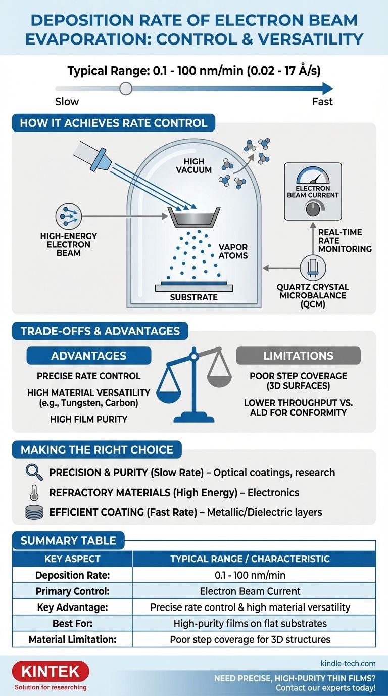
In practice, the deposition rate for electron beam (e-beam) evaporation is highly controllable, typically ranging from 0.1 to 100 nanometers per minute (nm/min). This wide operational window, which translates to approximately 0.02 to 17 Angstroms per second (Å/s), allows for both meticulous, slow-growth processes and rapid, high-throughput coating. The key is that the rate isn't a fixed property but a tunable parameter central to the technique's power.
While the numbers provide a baseline, the true value of e-beam evaporation lies not in its absolute speed but in its unique combination of precise rate control, material versatility, and high film purity, which are often unattainable with other methods.
How E-Beam Evaporation Achieves Rate Control
The deposition rate in an e-beam system is a direct consequence of its fundamental design. It is not an arbitrary outcome but a precisely managed variable controlled by the energy delivered to the source material.
The Role of the Electron Beam
The heart of the process is a high-energy beam of electrons, often accelerated by voltages up to 10 kV.
This beam is magnetically guided to strike a target material (the evaporant) held in a crucible. The kinetic energy of the electrons is converted to intense, localized heat upon impact.
By adjusting the electron beam's current, you directly control the power delivered to the material. A higher current results in more heat, a higher vapor pressure, and therefore a faster deposition rate.
The Necessity of High Vacuum
E-beam evaporation is performed under high vacuum conditions. This serves two critical purposes.
First, the vacuum minimizes contamination by removing ambient gas molecules that could otherwise become incorporated into the growing film, ensuring high purity.
Second, it allows the evaporated material atoms to travel in a straight, unimpeded "line-of-sight" path from the source to the substrate, maximizing deposition efficiency.
Real-Time Rate Monitoring
Most modern e-beam systems incorporate a feedback loop, typically using a quartz crystal microbalance (QCM).
The QCM measures the mass being added to its surface in real-time, which correlates directly to the deposition rate. This information is fed back to the e-beam controller, which automatically adjusts the beam current to maintain the desired rate with exceptional precision.
Understanding the Trade-offs
No deposition technique is perfect for every scenario. Choosing e-beam evaporation requires understanding its advantages in the context of its limitations.
Rate vs. Other Deposition Methods
Compared to sputtering, e-beam can often achieve higher deposition rates, especially for certain metals. However, sputtering can sometimes offer better film density and adhesion.
Compared to Atomic Layer Deposition (ALD), which builds films one atomic layer at a time, e-beam is orders of magnitude faster. The trade-off is that ALD provides unparalleled conformity and thickness control, which e-beam cannot match.
Unmatched Material Versatility
The intense, localized heating of the electron beam is its greatest strength.
It can evaporate materials with extremely high melting points, such as tungsten, tantalum, and carbon (graphite), which are impossible to deposit with simpler thermal evaporation methods. This makes e-beam essential for applications in advanced electronics and high-temperature optics.
Line-of-Sight Limitation
Because the vapor travels in a straight line, e-beam evaporation provides poor "step coverage." It cannot effectively coat the sidewalls of deep trenches or complex, three-dimensional surfaces.
This makes it best suited for depositing films on relatively flat substrates like wafers, glass plates, or optical components.
Making the Right Choice for Your Goal
Selecting e-beam evaporation depends entirely on your specific material requirements and application geometry.
- If your primary focus is precision and film purity: The slow-rate capability (down to 0.1 nm/min) and high-vacuum environment make e-beam ideal for creating complex optical coatings or research-grade electronic devices.
- If your primary focus is depositing refractory or dielectric materials: The high energy of the electron beam makes it one of the few, and often the best, methods for depositing high-melting-point materials.
- If your primary focus is efficient coating of flat surfaces: The higher end of the deposition rate (~100 nm/min) allows for cost-effective, high-throughput production of metallic and dielectric layers.
Ultimately, understanding the controllable rate of electron beam evaporation is key to leveraging its unique capabilities for the most demanding thin-film applications.
Summary Table:
| Key Aspect | Typical Range / Characteristic |
|---|---|
| Deposition Rate | 0.1 - 100 nm/min (0.02 - 17 Å/s) |
| Primary Control | Electron Beam Current |
| Key Advantage | Precise rate control & high material versatility |
| Best For | High-purity films on flat substrates |
| Material Limitation | Poor step coverage for 3D structures |
Need precise, high-purity thin films for your lab? KINTEK specializes in advanced lab equipment, including electron beam evaporation systems. Our solutions deliver the exact deposition control and material versatility your research or production demands. Contact our experts today to discuss how we can enhance your thin-film processes!
Visual Guide
Related Products
- Electron Beam Evaporation Coating Oxygen-Free Copper Crucible and Evaporation Boat
- Electron Beam Evaporation Coating Tungsten Crucible and Molybdenum Crucible for High Temperature Applications
- Electron Beam Evaporation Coating Conductive Boron Nitride Crucible BN Crucible
- Electron Beam Evaporation Coating Gold Plating Tungsten Molybdenum Crucible for Evaporation
- RF PECVD System Radio Frequency Plasma-Enhanced Chemical Vapor Deposition RF PECVD
People Also Ask
- What is the container that holds the metal source material called in e-beam evaporation? Ensure Purity and Quality in Your Thin-Film Deposition
- What is e-beam evaporation? Achieve High-Purity Thin Film Deposition for Your Lab
- What is the temperature of e-beam evaporation? Mastering the Two-Zone Thermal Process for Precision Films
- What is the deposition rate of e-beam evaporation? Control Thin Film Quality and Speed
- What is e-beam evaporation used for? Precision Coating for Optics, Aerospace & Electronics


