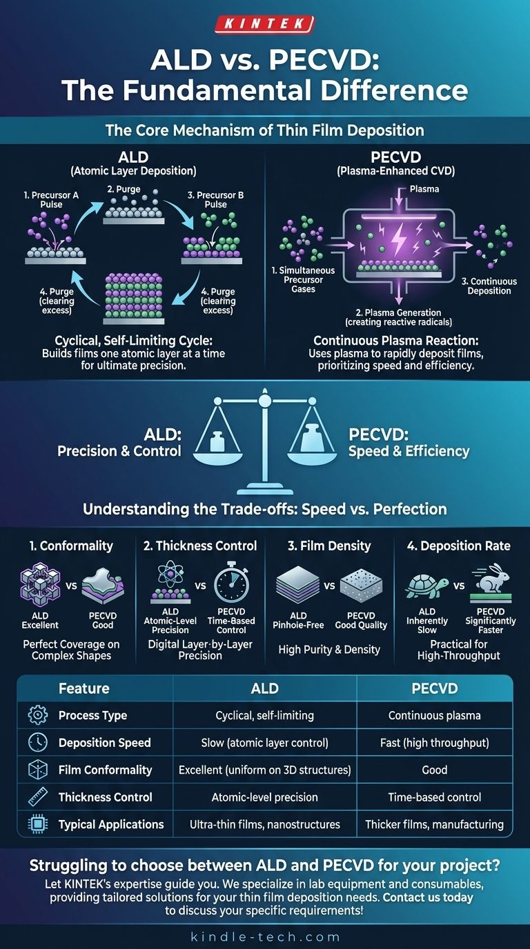
The fundamental difference between Atomic Layer Deposition (ALD) and Plasma-Enhanced Chemical Vapor Deposition (PECVD) lies in their core mechanism. ALD is a cyclical, self-limiting process that builds films one atomic layer at a time for ultimate precision, whereas PECVD is a continuous process that uses plasma to rapidly deposit films, prioritizing speed and efficiency.
The decision between ALD and PECVD is a classic engineering trade-off. You must choose between the near-perfect, atomic-level control of ALD and the practical, high-speed deposition of PECVD.
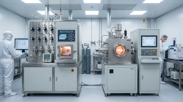
The Fundamental Difference: Process Mechanism
While both are forms of Chemical Vapor Deposition (CVD), their methods for creating a film are fundamentally distinct. This difference in mechanism is the source of all their respective strengths and weaknesses.
ALD: The Self-Limiting Cycle
ALD operates by separating the chemical reaction into two distinct half-reactions. It uses sequential pulses of precursor gases, with a purge step in between.
First, a pulse of the first precursor gas is introduced, which reacts with the substrate surface until every available reaction site is occupied. The process is self-limiting; the reaction naturally stops after one complete molecular layer is formed.
Excess gas is purged, and a second precursor is pulsed in. This second gas reacts only with the first layer, completing the film's chemical composition for that single atomic layer. This cycle is repeated to build the film with digital, layer-by-layer precision.
PECVD: The Continuous Plasma Reaction
In contrast, PECVD is a continuous process. All necessary precursor gases are introduced into the chamber simultaneously.
Instead of relying solely on high temperatures like conventional CVD, PECVD uses an energy source to generate plasma. This plasma energizes the gas mixture, breaking down the precursor molecules into reactive radicals.
These radicals then react on the substrate surface, continuously depositing the film. The film thickness is primarily controlled by the duration of the process.
How This Impacts Film Quality and Control
The difference between a cyclical, self-limiting process and a continuous one has profound implications for the final film's characteristics.
Conformality: The ALD Advantage
Conformality refers to a film's ability to coat complex, three-dimensional structures with a perfectly uniform thickness.
Because the ALD process is governed by surface reactions, it produces exceptionally conformal films. The gas precursors will find and react with every available site, regardless of the surface's geometry, resulting in perfect coverage on deep trenches and complex shapes.
Thickness Control: Atomic-Level Precision
ALD offers the highest possible level of thickness control. Since each cycle deposits a known, fixed amount of material (typically a fraction of a nanometer), you can determine the final film thickness simply by counting the number of cycles. This is true digital control.
PECVD thickness is controlled by time, pressure, and gas flow, which is less precise and subject to minor variations.
Film Density and Purity
The slow, methodical nature of ALD typically results in highly dense, pinhole-free films with very low impurity levels. The self-limiting reactions and purge steps ensure a very clean and well-structured deposition.
Understanding the Trade-offs: Speed vs. Perfection
Choosing the right technique requires a clear understanding of your project's priorities, as the "perfect" film from ALD comes at a significant cost.
The Cost of Precision: Deposition Rate
This is the most critical trade-off. ALD is inherently slow. Building a film one atomic layer at a time is a time-consuming process, making it impractical for applications requiring thick films (e.g., several microns).
PECVD is significantly faster. Its continuous, plasma-driven nature allows for much higher deposition rates, making it the workhorse for applications where throughput and efficiency are key.
Low-Temperature Processing
Both techniques are considered low-temperature processes compared to conventional thermal CVD, which often requires 600-800°C.
PECVD operates from room temperature up to around 350°C. ALD typically operates in a similar, low-temperature window. This makes both suitable for coating temperature-sensitive substrates.
Scalability and Cost
For applications requiring thicker films, PECVD is generally more cost-effective and scalable due to its high deposition rate. The long process times of ALD can make it prohibitively expensive for anything other than ultra-thin film applications where its unique properties are essential.
Making the Right Choice for Your Goal
Your application's specific requirements will dictate the correct choice. Evaluate your priorities based on the following outcomes.
- If your primary focus is ultimate precision and conformality on 3D nanostructures: ALD is the only technique that provides the necessary atomic-level control.
- If your primary focus is depositing thicker films (hundreds of nanometers to microns) quickly and efficiently: PECVD offers the necessary speed and scalability for manufacturing.
- If you need a high-quality barrier or dielectric layer and speed is a factor: PECVD is often the more practical and economical choice, providing good quality films at a much higher throughput.
Ultimately, selecting the right deposition method is about aligning the unique capabilities of the technique with the non-negotiable requirements of your project.
Summary Table:
| Feature | ALD (Atomic Layer Deposition) | PECVD (Plasma-Enhanced CVD) |
|---|---|---|
| Process Type | Cyclical, self-limiting | Continuous plasma reaction |
| Deposition Speed | Slow (atomic layer control) | Fast (high throughput) |
| Film Conformality | Excellent (uniform on 3D structures) | Good |
| Thickness Control | Atomic-level precision | Time-based control |
| Typical Applications | Ultra-thin films, nanostructures | Thicker films, manufacturing |
Struggling to choose between ALD and PECVD for your project? Let KINTEK's expertise guide you. We specialize in lab equipment and consumables, providing tailored solutions for your thin film deposition needs. Our team can help you select the right technology to achieve optimal film quality, efficiency, and cost-effectiveness for your laboratory. Contact us today to discuss your specific requirements and discover how KINTEK can enhance your research and production processes!
Visual Guide
Related Products
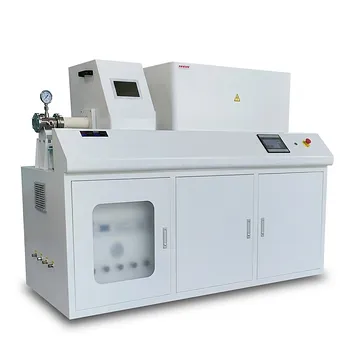
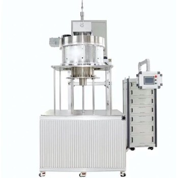
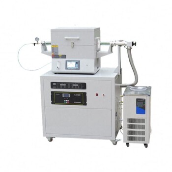
- Chemical Vapor Deposition CVD Equipment System Chamber Slide PECVD Tube Furnace with Liquid Gasifier PECVD Machine
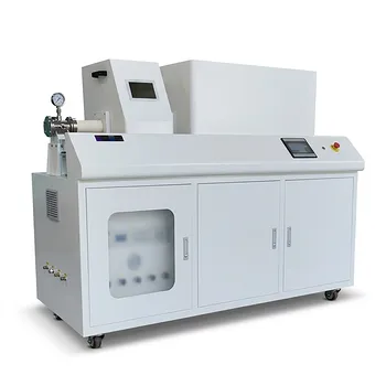
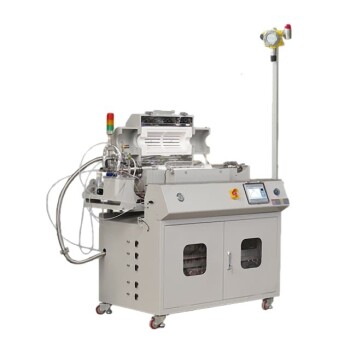
- Inclined Rotary Plasma Enhanced Chemical Vapor Deposition PECVD Equipment Tube Furnace Machine
- Inclined Rotary Plasma Enhanced Chemical Vapor Deposition PECVD Equipment Tube Furnace Machine
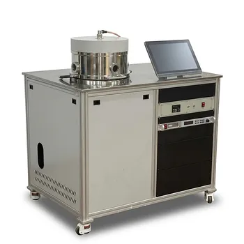
- RF PECVD System Radio Frequency Plasma-Enhanced Chemical Vapor Deposition RF PECVD
- Aluminized Ceramic Evaporation Boat for Thin Film Deposition
People Also Ask
- What are the core advantages of PE-CVD in OLED encapsulation? Protect Sensitive Layers with Low-Temp Film Deposition
- What happens during deposition chemistry? Building Thin Films from Gaseous Precursors
- What is plasma enhanced chemical vapor deposition PECVD equipment? A Guide to Low-Temperature Thin Film Deposition
- What types of substrates are used in CVD to facilitate graphene films? Optimize Graphene Growth with the Right Catalyst
- What are the advantages of chemical vapor deposition? Achieve Superior Thin Films for Your Lab
