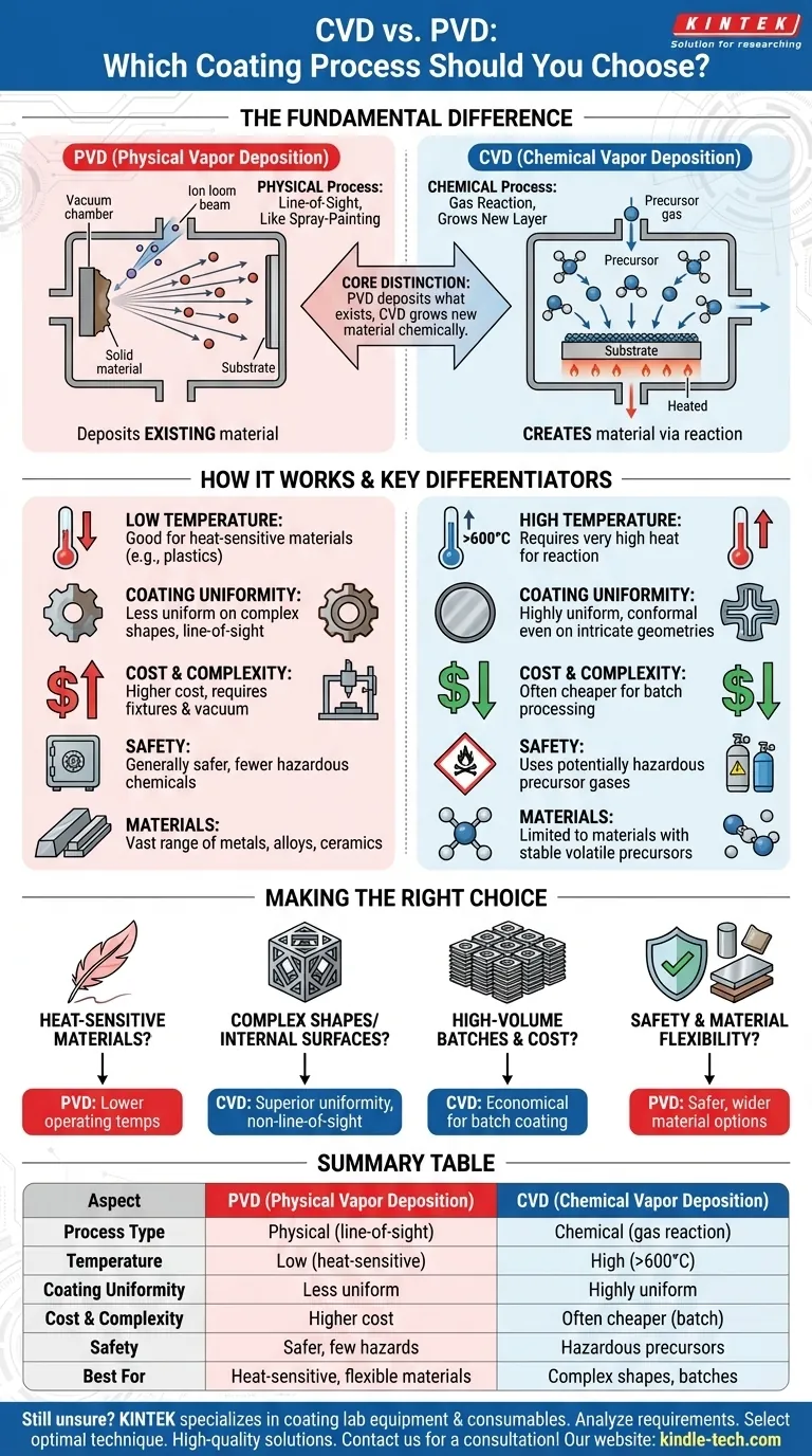
The fundamental difference between Chemical Vapor Deposition (CVD) and Physical Vapor Deposition (PVD) lies in how the coating material reaches and forms a film on a substrate. PVD is a physical process, akin to spray-painting with atoms in a vacuum, where the material is physically blasted or evaporated onto a surface. In contrast, CVD is a chemical process where precursor gases react on a heated surface to "grow" a new layer, molecule by molecule.
The core distinction to remember is that PVD deposits material that already exists, while CVD creates the material directly on the substrate through a chemical reaction. This single difference dictates the process temperature, coating uniformity, cost, and suitable applications for each method.
How Does Each Process Fundamentally Work?
To understand when to use each technique, we must first grasp their distinct mechanisms. One relies on physical force and line-of-sight, while the other relies on a pervasive chemical environment.
Physical Vapor Deposition (PVD): A Line-of-Sight Process
PVD encompasses a family of techniques where a solid material is converted into a vapor and then condensed onto a substrate inside a vacuum chamber.
This is a purely physical mechanism. Common methods include heating a material until it evaporates or bombarding it with ions to knock atoms loose. These atoms then travel in a straight line and deposit on any surface in their path.
Chemical Vapor Deposition (CVD): A Chemical Reaction Process
CVD is fundamentally a chemical manufacturing process that happens at a microscopic scale.
It involves introducing volatile precursor gases into a reaction chamber containing a heated substrate. The heat triggers a chemical reaction among the gases, causing a solid film to form—or deposit—on the substrate's surface. Unwanted chemical by-products are then vented away.
Key Differentiators in Practice
The difference between a physical and chemical process creates significant practical consequences for temperature, coverage, and material compatibility.
Operating Temperature
This is often the most critical deciding factor. CVD typically requires very high temperatures (often >600°C) to drive the necessary chemical reactions on the substrate's surface.
PVD is a much lower-temperature process, as it does not rely on chemical reactions. This makes PVD the only viable option for coating materials that cannot withstand the intense heat of CVD, such as many plastics or heat-treated steels.
Coating Uniformity and Coverage
Because PVD is a "line-of-sight" technique, it struggles to evenly coat complex shapes, sharp corners, or internal surfaces. The coating is thickest on areas directly facing the vapor source.
CVD, however, excels at this. Since the precursor gases envelop the entire substrate, the chemical reaction occurs on all heated surfaces simultaneously. This provides a highly uniform and conformal coating, even inside deep holes or on intricate geometries.
Film Quality and Material Options
The resulting film structures differ. PVD coatings tend to have fewer voids, which can be an advantage for certain applications requiring high density.
Material choice is also constrained by the process. PVD can deposit a vast range of metals, alloys, and ceramics. CVD is limited to materials for which stable, volatile precursor gases are available and safe to handle.
Understanding the Trade-offs
Choosing between PVD and CVD requires an objective look at their respective costs, complexities, and safety profiles.
The Cost and Complexity Equation
Generally, CVD is the cheaper process for batch applications. Its ability to uniformly coat many parts at once, regardless of their complexity, makes it highly efficient.
PVD is often more expensive, partly due to the complex fixtures required to hold and rotate parts to ensure adequate coverage. The vacuum technology and power sources can also add to the cost.
Handling and Safety
PVD is often considered a safer and cleaner process. It does not typically involve the use of toxic or corrosive precursor gases.
The chemical precursors used in CVD can be hazardous, requiring specialized handling, storage, and exhaust systems to manage toxic by-products.
Making the Right Choice for Your Application
The optimal choice is not about which process is "better" but which is best suited for your specific substrate, geometry, and performance goals.
- If your primary focus is coating heat-sensitive materials: PVD is the definitive choice due to its significantly lower operating temperatures.
- If your primary focus is achieving uniform coverage on complex shapes: CVD's gas-based, non-line-of-sight nature makes it far superior for intricate geometries and internal surfaces.
- If your primary focus is cost-effectiveness for high-volume batches: CVD is often the more economical solution for uniformly coating many parts at once.
- If your primary focus is process safety and material flexibility: PVD avoids many of the hazardous chemicals associated with CVD and can deposit a wider range of existing alloys.
Ultimately, understanding these core principles empowers you to select the deposition technique that aligns perfectly with your engineering requirements.
Summary Table:
| Aspect | PVD (Physical Vapor Deposition) | CVD (Chemical Vapor Deposition) |
|---|---|---|
| Process Type | Physical (line-of-sight) | Chemical (gas reaction) |
| Temperature | Low temperature (good for heat-sensitive materials) | High temperature (>600°C) |
| Coating Uniformity | Less uniform on complex shapes | Highly uniform, even on intricate geometries |
| Cost & Complexity | Higher cost, complex fixtures | Often cheaper for batch processing |
| Safety | Generally safer, fewer hazardous chemicals | Uses potentially hazardous precursor gases |
| Best For | Heat-sensitive materials, material flexibility | Complex shapes, high-volume batches |
Still unsure whether PVD or CVD is right for your specific application?
At KINTEK, we specialize in lab equipment and consumables for all your coating and deposition needs. Our experts can help you:
- Analyze your substrate and performance requirements
- Select the optimal deposition technique for your project
- Provide high-quality equipment and consumables tailored to your lab's workflow
Don't leave your coating results to chance. Contact our team today for a personalized consultation and discover how KINTEK can enhance your laboratory's capabilities and efficiency!
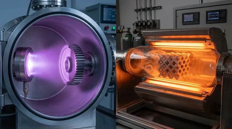
Visual Guide
Related Products
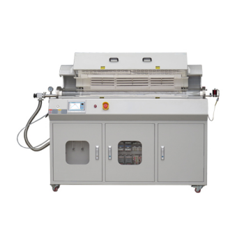
- Chemical Vapor Deposition CVD Equipment System Chamber Slide PECVD Tube Furnace with Liquid Gasifier PECVD Machine
- Inclined Rotary Plasma Enhanced Chemical Vapor Deposition PECVD Equipment Tube Furnace Machine
- RF PECVD System Radio Frequency Plasma-Enhanced Chemical Vapor Deposition RF PECVD
- Customer Made Versatile CVD Tube Furnace Chemical Vapor Deposition Chamber System Equipment
- Vacuum Hot Press Furnace Machine for Lamination and Heating
People Also Ask
- What is the difference between CVD and PECVD? Choose the Right Thin-Film Deposition Method
- How are PECVD and CVD different? A Guide to Choosing the Right Thin-Film Deposition Process
- How is PECVD different from CVD? Unlock Low-Temperature Thin Film Deposition
- What is the difference between CVD and PVD process? A Guide to Choosing the Right Coating Method
- What is the difference between thermal CVD and PECVD? Choose the Right Thin-Film Deposition Method