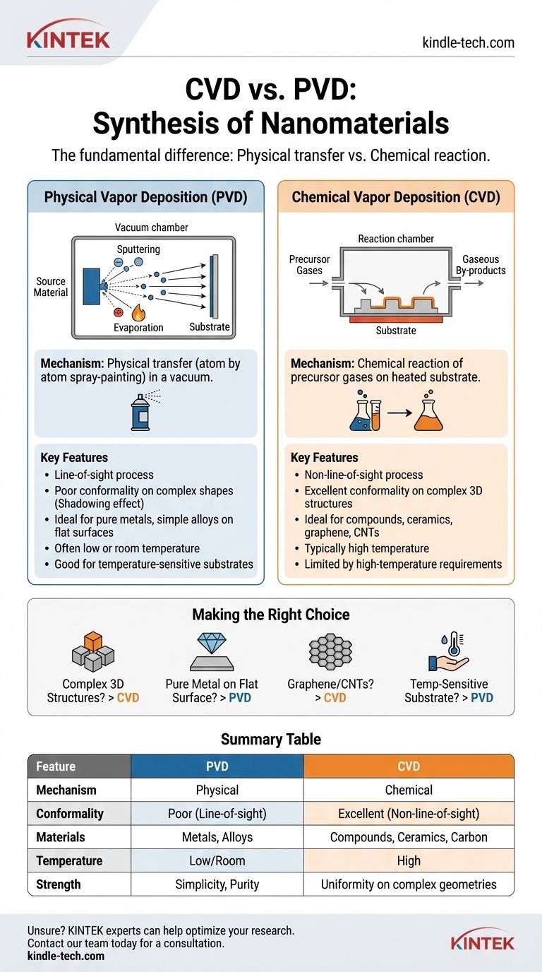
The fundamental difference between Chemical Vapor Deposition (CVD) and Physical Vapor Deposition (PVD) lies in how the material travels to and forms on the substrate. PVD is a physical process, akin to spray-painting with atoms, where a solid material is vaporized and then condenses onto a surface. In contrast, CVD is a chemical process where precursor gases react on the substrate's surface to grow the desired material, leaving behind gaseous by-products.
Your choice between these methods is not about which is universally "better," but which mechanism—a physical transfer or a chemical reaction—best suits your material, the geometry of your substrate, and the specific properties you need to achieve in the final nanomaterial.
The Core Mechanism: Physical vs. Chemical
The names "Physical Vapor Deposition" and "Chemical Vapor Deposition" are not arbitrary; they describe the fundamental state of the material being deposited. Understanding this distinction is the key to selecting the correct method.
How Physical Vapor Deposition (PVD) Works
PVD is a line-of-sight process that occurs in a vacuum. The core idea is to physically liberate atoms or molecules from a solid source and have them travel in a straight line to coat a substrate.
The source material is converted into a vapor through purely physical means, such as sputtering (bombarding the source with ions) or thermal evaporation (heating the source until it vaporizes). These vaporized particles then travel through the vacuum chamber and condense on the cooler substrate, forming a thin, pure film.
How Chemical Vapor Deposition (CVD) Works
CVD does not start with the final material in solid form. Instead, it uses one or more volatile precursor gases that contain the required atoms.
These gases are introduced into a reaction chamber where they decompose or react with each other on and near a heated substrate. This chemical reaction forms the desired solid material directly on the surface, while waste products are removed by a continuous gas flow.
Key Differentiators in Practice
The difference between a physical transfer and a chemical reaction creates significant practical consequences for the synthesis of nanomaterials.
Coating Conformality and Geometry
This is arguably the most significant practical difference. Because PVD is a line-of-sight technique, it struggles to coat complex, non-flat surfaces. Any area not in the direct path of the vapor source will receive little to no coating, an effect known as "shadowing."
CVD, however, is not limited by line-of-sight. The precursor gases can flow into and around complex 3D structures, deep holes, or shaded areas, allowing for a highly uniform and conformal coating on all exposed surfaces.
Material and Precursor Options
PVD is excellent for depositing materials that can be easily vaporized, such as pure metals and certain alloys. Its range is limited to elements that can be effectively targeted by sputtering or evaporation.
CVD excels where PVD cannot. It can be used to deposit materials from elements that are very difficult to evaporate, as long as a suitable volatile chemical compound exists. This makes it ideal for producing complex compounds, ceramics, and specific carbon nanostructures like graphene and carbon nanotubes.
Process Conditions and Purity
PVD almost always requires a high vacuum to allow particles to travel without colliding with ambient gas molecules. This ensures a very pure coating, as contaminants are minimized.
CVD can be performed under a wider range of pressures, from low pressure to atmospheric pressure. The purity of a CVD film is determined by the purity of the precursor gases and the precision with which the chemical reaction can be controlled.
Understanding the Trade-offs and Limitations
Neither technique is a universal solution. Your decision must be informed by their inherent limitations.
The Challenge of PVD: Coverage and Complexity
The primary drawback of PVD is its poor conformality on complex shapes. It is fundamentally a surface-coating technique for relatively simple geometries. Creating complex compound films also requires multiple sources, which adds complexity.
The Challenge of CVD: Chemistry and Safety
The strength of CVD—its reliance on chemistry—is also its main challenge. The precursor gases can be highly toxic, corrosive, or flammable, requiring significant safety protocols. The chemical reactions can be complex to control, and unwanted by-products can sometimes contaminate the film.
Temperature and Substrate Compatibility
CVD processes often require high substrate temperatures to provide the necessary activation energy for the chemical reactions to occur. This can make it unsuitable for coating temperature-sensitive substrates, such as certain polymers. Many PVD techniques can be performed at or near room temperature, offering much greater substrate flexibility.
Making the Right Choice for Your Goal
Select your method based on the primary requirement of your application.
- If your primary focus is coating complex 3D structures uniformly: CVD is the only viable choice due to its non-line-of-sight deposition.
- If your primary focus is depositing a pure elemental metal or a simple alloy onto a flat surface: PVD is often the simpler, faster, and more direct method.
- If your primary focus is growing specific, highly crystalline structures like graphene sheets or carbon nanotube arrays: CVD is the dominant industrial method, as it builds the material through controlled chemical reactions.
- If your primary focus is coating a temperature-sensitive substrate: PVD is generally the safer choice, as many of its variants can operate at significantly lower temperatures than CVD.
Ultimately, your choice is dictated not by the material alone, but by the geometry and chemical precision your application demands.
Summary Table:
| Feature | PVD (Physical Vapor Deposition) | CVD (Chemical Vapor Deposition) |
|---|---|---|
| Mechanism | Physical transfer (sputtering/evaporation) | Chemical reaction on substrate surface |
| Coating Conformality | Line-of-sight; poor for complex 3D shapes | Non-line-of-sight; excellent for complex 3D shapes |
| Material Options | Pure metals, simple alloys | Complex compounds, ceramics, graphene, carbon nanotubes |
| Process Temperature | Often low or room temperature | Typically high temperature |
| Substrate Compatibility | Good for temperature-sensitive materials | Limited by high-temperature requirements |
| Primary Strength | Simplicity, purity for flat surfaces | Uniformity on complex geometries, versatile materials |
Still unsure whether CVD or PVD is right for your lab's specific application?
At KINTEK, we specialize in providing advanced lab equipment and consumables tailored to your nanomaterial synthesis needs. Our experts can help you select the perfect system to achieve precise coatings, whether you're working with complex 3D structures or temperature-sensitive substrates.
Let us help you optimize your research and production processes.
Contact our team today for a personalized consultation and discover how KINTEK's solutions can enhance your laboratory's capabilities.
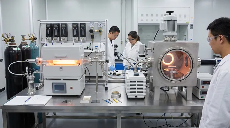
Visual Guide
Related Products
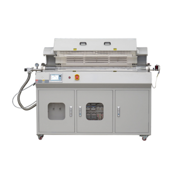
- Chemical Vapor Deposition CVD Equipment System Chamber Slide PECVD Tube Furnace with Liquid Gasifier PECVD Machine
- Inclined Rotary Plasma Enhanced Chemical Vapor Deposition PECVD Equipment Tube Furnace Machine
- RF PECVD System Radio Frequency Plasma-Enhanced Chemical Vapor Deposition RF PECVD
- Customer Made Versatile CVD Tube Furnace Chemical Vapor Deposition Chamber System Equipment
- Vacuum Hot Press Furnace Machine for Lamination and Heating
People Also Ask
- How is PECVD different from CVD? Unlock Low-Temperature Thin Film Deposition
- What are the advantages of PECVD over CVD? Achieve High-Quality Thin Films at Lower Temperatures
- How plasma is generated in PECVD? A Step-by-Step Breakdown of the Process
- What is the difference between CVD and PVD process? A Guide to Choosing the Right Coating Method
- What are the examples of CVD method? Discover the Versatile Applications of Chemical Vapor Deposition