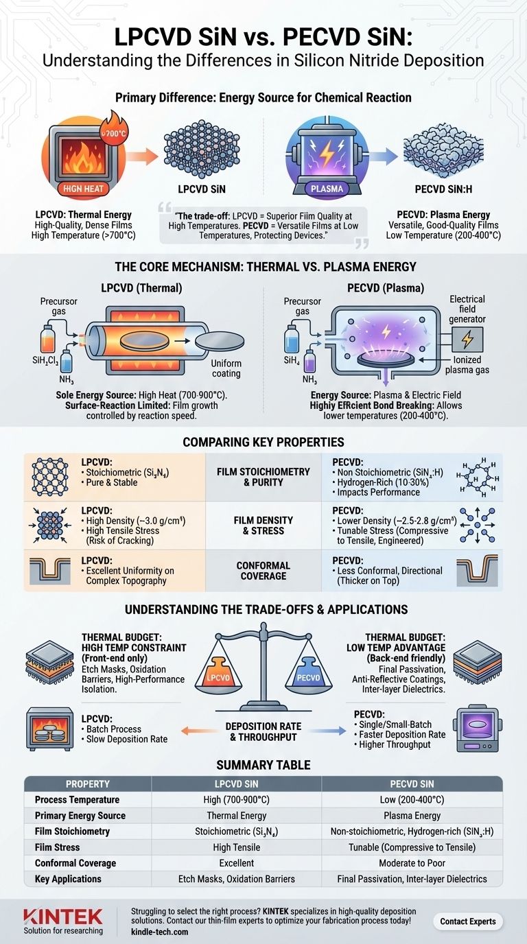
At their core, the primary difference between LPCVD and PECVD for depositing silicon nitride (SiN) is the energy source used to drive the chemical reaction. Low-Pressure Chemical Vapor Deposition (LPCVD) relies on high thermal energy (typically >700°C), resulting in high-quality, dense films. In contrast, Plasma-Enhanced Chemical Vapor Deposition (PECVD) uses plasma to dissociate precursor gases at much lower temperatures (typically 200-400°C), making it suitable for temperature-sensitive substrates.
The decision between LPCVD and PECVD for silicon nitride is fundamentally a trade-off between film quality and thermal budget. LPCVD provides superior films at the cost of high temperatures, while PECVD offers versatile, good-quality films at temperatures low enough to protect underlying device structures.
The Core Mechanism: Thermal vs. Plasma Energy
Both LPCVD and PECVD are forms of Chemical Vapor Deposition (CVD), where precursor gases react to form a solid thin film on a substrate. The key distinction lies in how they supply the energy needed to break the chemical bonds of those gases.
LPCVD: The High-Temperature Approach
LPCVD uses high heat in a low-pressure furnace as the sole energy source.
Precursor gases, typically dichlorosilane (SiH₂Cl₂) and ammonia (NH₃), are introduced into the furnace. The high temperature (700-900°C) provides the thermal energy necessary to initiate the surface chemical reactions that form silicon nitride.
This process is surface-reaction limited, meaning the film growth rate is controlled by the reaction speed on the wafer surface, not by how fast gas can get there.
PECVD: The Low-Temperature Alternative
PECVD uses an electrical field to generate plasma inside the reaction chamber.
This plasma, a high-energy ionized gas, bombards the precursor molecules (often silane (SiH₄) and ammonia (NH₃)). This energy transfer is highly efficient at breaking chemical bonds without needing extreme heat.
The deposition can therefore proceed at much lower temperatures (200-400°C), protecting temperature-sensitive materials like aluminum interconnects already on the wafer.
Comparing Key Film and Process Properties
The difference in energy source leads to significant and predictable variations in the final silicon nitride film and the deposition process itself.
Film Stoichiometry and Purity
LPCVD produces a film that is almost perfectly stoichiometric (Si₃N₄). Due to the high temperature, hydrogen from the ammonia precursor is driven off, resulting in a very pure and stable film.
PECVD films are inherently non-stoichiometric and are more accurately described as SiNₓ:H. They contain a significant amount of bonded hydrogen (often 10-30%), which can impact electrical performance and stability.
Film Density and Stress
LPCVD films are very dense (typically ~3.0 g/cm³) and possess a high intrinsic tensile stress. This high stress can be a limiting factor for thick films, which may crack.
PECVD films are less dense (~2.5-2.8 g/cm³), and critically, their stress can be engineered. By adjusting process parameters like RF power and pressure, the film stress can be tuned from compressive to tensile, a major advantage for device manufacturing.
Conformal Coverage
LPCVD provides excellent conformality. Because the reaction is slow and surface-limited, the film deposits uniformly over highly complex, three-dimensional surface topographies.
PECVD coverage is significantly less conformal and can be somewhat directional. The reaction depends on the arrival of reactive species from the plasma, leading to thicker films on top surfaces than on sidewalls.
Understanding the Trade-offs
Choosing between these methods requires a clear understanding of their fundamental limitations and advantages.
The Thermal Budget Constraint
The high temperature of LPCVD is its single greatest drawback. It cannot be used after low-melting-point materials (like aluminum) have been deposited on the wafer. Its use is largely restricted to "front-end" fabrication steps.
The low temperature of PECVD is its primary advantage. It makes it the default choice for "back-end" processes like final device passivation, where the thermal budget is extremely limited.
Deposition Rate and Throughput
LPCVD is a batch process, where hundreds of wafers are processed simultaneously in a furnace tube. However, the deposition rate on each wafer is slow.
PECVD is typically a single-wafer or small-batch process, but its deposition rate is much higher than LPCVD. For many applications, this leads to better overall factory throughput.
Quality vs. Application Suitability
LPCVD SiN is the gold standard for applications demanding the highest quality, such as etch masks, oxidation barriers, and high-performance electrical isolation.
PECVD SiN is a versatile workhorse for applications where perfection is not required but low temperature is critical. It excels as a final passivation layer (protecting from moisture and damage), an anti-reflective coating, and an inter-layer dielectric.
Making the Right Choice for Your Application
Your choice is dictated by the specific requirements of your process step and device architecture.
- If your primary focus is maximum film quality and thermal stability: LPCVD is the definitive choice for its stoichiometric, dense, and low-hydrogen films.
- If your primary focus is depositing on a temperature-sensitive substrate: PECVD is the only viable option due to its low-temperature, plasma-driven process.
- If your primary focus is tunable film stress or high throughput: PECVD offers significant advantages in controlling film stress and provides a much faster deposition rate.
- If your primary focus is perfect conformal coating over complex topography: LPCVD provides vastly superior step coverage essential for applications like trench isolation.
Ultimately, selecting the right silicon nitride deposition method depends on a clear understanding of your device's thermal limitations and final performance requirements.
Summary Table:
| Property | LPCVD SiN | PECVD SiN |
|---|---|---|
| Process Temperature | High (700-900°C) | Low (200-400°C) |
| Primary Energy Source | Thermal Energy | Plasma Energy |
| Film Stoichiometry | Stoichiometric (Si₃N₄) | Non-stoichiometric, Hydrogen-rich (SiNₓ:H) |
| Film Stress | High Tensile | Tunable (Compressive to Tensile) |
| Conformal Coverage | Excellent | Moderate to Poor |
| Key Applications | Etch Masks, Oxidation Barriers | Final Passivation, Inter-layer Dielectrics |
Struggling to select the right silicon nitride deposition process for your semiconductor or MEMS device? The choice between LPCVD and PECVD is critical for your device's performance and yield. KINTEK specializes in providing high-quality lab equipment and consumables for precise thin-film deposition. Our experts can help you navigate these trade-offs to achieve optimal results for your specific application, whether it requires the ultimate film quality of LPCVD or the low-temperature versatility of PECVD.
Let's optimize your fabrication process together. Contact our thin-film experts today!
Visual Guide
Related Products
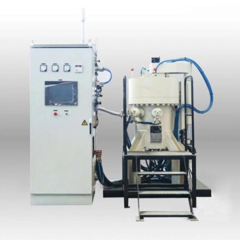
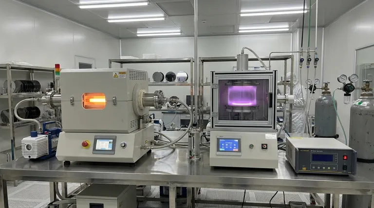
- Inclined Rotary Plasma Enhanced Chemical Vapor Deposition PECVD Equipment Tube Furnace Machine
- Chemical Vapor Deposition CVD Equipment System Chamber Slide PECVD Tube Furnace with Liquid Gasifier PECVD Machine
- Inclined Rotary Plasma Enhanced Chemical Vapor Deposition PECVD Equipment Tube Furnace Machine
- Precision Machined Silicon Nitride (SiN) Ceramic Sheet for Engineering Advanced Fine Ceramics
- RF PECVD System Radio Frequency Plasma-Enhanced Chemical Vapor Deposition RF PECVD
People Also Ask
- What are the benefits of plasma enhanced CVD? Achieve High-Quality, Low-Temperature Film Deposition
- What is plasma enhanced chemical vapor deposition PECVD equipment? A Guide to Low-Temperature Thin Film Deposition
- What is plasma enhanced chemical vapour deposition PECVD used for? Enable Low-Temp Thin Films for Electronics & Solar
- How does PECVD equipment facilitate the directional growth of carbon nanotubes? Achieve Precision Vertical Alignment
- Why is a PECVD system required for vertical graphene synthesis? Master Directional Control for 3D Nanostructures