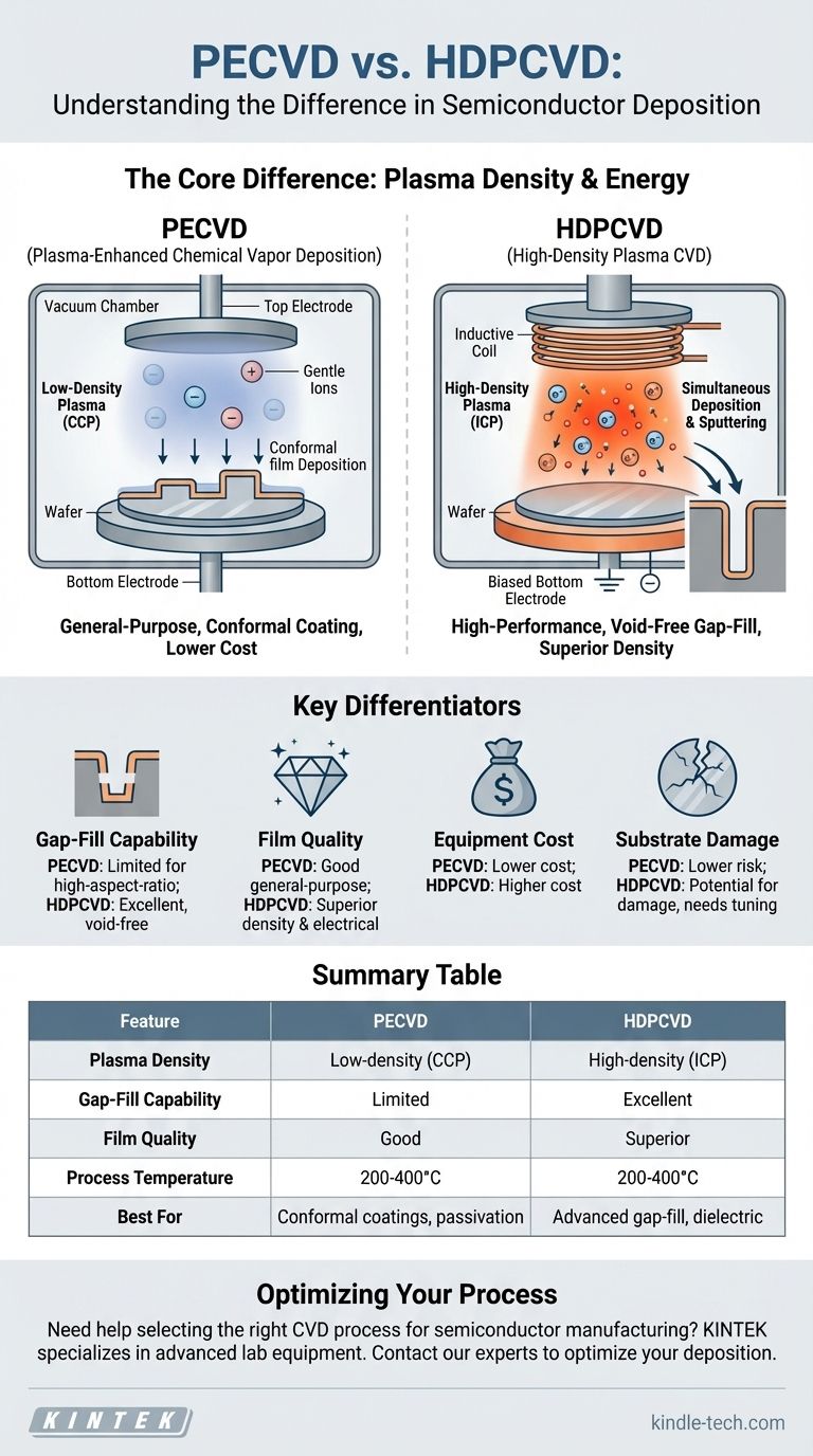
At its core, the difference between PECVD and HDPCVD lies in the plasma used to deposit the film. High-Density Plasma CVD (HDPCVD) is an advanced form of Plasma-Enhanced CVD (PECVD) that uses a much denser, more energetic plasma. This fundamental difference allows HDPCVD to simultaneously deposit material and sputter it with ions, resulting in significantly higher quality films ideal for filling challenging, microscopic gaps.
While both are low-temperature chemical vapor deposition techniques, PECVD is a general-purpose workhorse for depositing films, whereas HDPCVD is a specialized, high-performance process engineered for superior film density and exceptional gap-fill capabilities in advanced semiconductor manufacturing.
The Foundation: Understanding PECVD
PECVD, or Plasma-Enhanced Chemical Vapor Deposition, is a foundational process in modern electronics manufacturing. It solves a major limitation of purely thermal CVD methods which require very high temperatures that can damage underlying components.
How It Works
PECVD introduces precursor gases into a vacuum chamber and uses an electric field to generate a plasma, which is an energized state of gas. This plasma provides the energy needed to break down the gas molecules and deposit a thin film onto a substrate, all at a much lower temperature (typically 200-400°C).
The Role of the Plasma
The plasma in a standard PECVD system is a low-density plasma. It is typically generated using a technique called capacitively coupled plasma (CCP), where the substrate sits on one electrode and another electrode is placed opposite it. This creates a relatively diffuse plasma sufficient for decomposing the precursor gases.
Key Characteristics
Standard PECVD is highly valued for its versatility and cost-effectiveness. It is excellent for depositing conformal dielectric and passivation layers, such as silicon dioxide (SiO₂) and silicon nitride (Si₃N₄), over existing structures on a wafer.
The Evolution: High-Density Plasma CVD (HDPCVD)
HDPCVD was developed to overcome the limitations of standard PECVD, particularly as the features on microchips became smaller and more tightly packed.
A Higher-Density Approach
The defining feature of HDPCVD is its use of a high-density plasma, which is typically generated using an inductively coupled plasma (ICP) source. This technique produces a plasma that is 100 to 1000 times more dense than the plasma in a standard PECVD system.
The Simultaneous Deposition and Sputter Effect
This high-density plasma enables HDPCVD's most critical feature. In addition to the plasma source, a separate RF bias is applied to the substrate holder. This bias attracts high-energy ions from the dense plasma, causing them to bombard the substrate.
The result is a process of simultaneous deposition and sputtering. As material deposits, the energetic ions continuously sputter away excess material, particularly from the corners and top edges of trenches, preventing voids from forming.
Superior Film Quality
The intense ion bombardment during deposition also creates films that are physically denser, have lower hydrogen content, and exhibit superior electrical properties compared to films from a standard PECVD process.
Understanding the Key Differences
The choice between PECVD and HDPCVD comes down to specific process requirements. The higher performance of HDPCVD is not always necessary and comes with clear trade-offs.
Plasma Generation and Density
PECVD uses a lower-density, capacitively coupled plasma (CCP). HDPCVD uses a much higher-density, inductively coupled plasma (ICP), which provides a higher concentration of reactive ions.
Gap-Fill Capability
This is the most significant differentiator. PECVD provides a conformal coating but struggles to fill high-aspect-ratio (deep and narrow) gaps without creating voids. HDPCVD excels at this, using its sputter component to achieve a "bottom-up" fill that is completely void-free.
Film Quality vs. Cost
HDPCVD produces denser, more stable films with better electrical characteristics. However, the equipment is significantly more complex and expensive than standard PECVD systems.
Potential for Substrate Damage
While the ion bombardment in HDPCVD is key to its benefits, it can also cause physical or electrical damage to sensitive device layers underneath. This requires careful process tuning. Standard PECVD is a gentler, lower-risk process in this regard.
Making the Right Choice for Your Goal
Selecting the correct deposition method requires a clear understanding of your application's geometric constraints and film quality requirements.
- If your primary focus is high-aspect-ratio gap fill: HDPCVD is the industry-standard and often the only viable choice, especially for applications like Shallow Trench Isolation (STI).
- If your primary focus is the highest quality dielectric film at low temperatures: HDPCVD provides superior density, stability, and electrical performance.
- If your primary focus is general-purpose conformal coating or passivation: Standard PECVD is the most reliable, well-understood, and cost-effective solution for less demanding geometries.
Ultimately, the evolution from PECVD to HDPCVD mirrors the evolution of the semiconductor industry itself—a relentless drive for smaller features that demands more advanced process solutions.
Summary Table:
| Feature | PECVD | HDPCVD |
|---|---|---|
| Plasma Density | Low-density (CCP) | High-density (ICP) |
| Gap-Fill Capability | Limited for high-aspect-ratio gaps | Excellent void-free fill |
| Film Quality | Good for general-purpose | Superior density & electrical properties |
| Process Temperature | 200-400°C | 200-400°C |
| Equipment Cost | Lower | Higher |
| Best For | Conformal coatings, passivation | Advanced semiconductor gap-fill |
Need help selecting the right CVD process for your semiconductor manufacturing? KINTEK specializes in advanced lab equipment and consumables for cutting-edge research and production. Our experts can help you choose between PECVD and HDPCVD solutions tailored to your specific gap-fill requirements and film quality needs. Contact our technical team today to optimize your deposition process and achieve superior results!
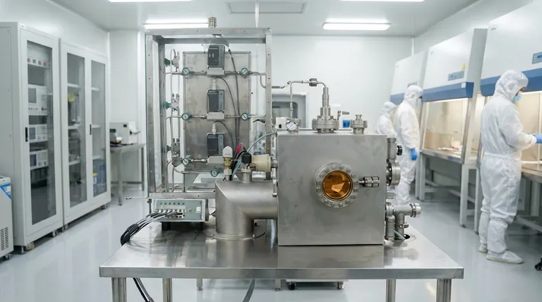
Visual Guide
Related Products
- Inclined Rotary Plasma Enhanced Chemical Vapor Deposition PECVD Equipment Tube Furnace Machine
- Chemical Vapor Deposition CVD Equipment System Chamber Slide PECVD Tube Furnace with Liquid Gasifier PECVD Machine
- Inclined Rotary Plasma Enhanced Chemical Vapor Deposition PECVD Equipment Tube Furnace Machine
- RF PECVD System Radio Frequency Plasma-Enhanced Chemical Vapor Deposition RF PECVD
- Multi Heating Zones CVD Tube Furnace Machine Chemical Vapor Deposition Chamber System Equipment
People Also Ask
- What are the benefits of plasma enhanced CVD? Achieve High-Quality, Low-Temperature Film Deposition
- How does PECVD equipment facilitate the directional growth of carbon nanotubes? Achieve Precision Vertical Alignment
- What is plasma enhanced chemical vapour deposition PECVD used for? Enable Low-Temp Thin Films for Electronics & Solar
- What is plasma enhanced chemical vapor deposition PECVD equipment? A Guide to Low-Temperature Thin Film Deposition
- How does plasma enhanced chemical vapor deposition work? Enable Low-Temperature Thin Film Deposition


