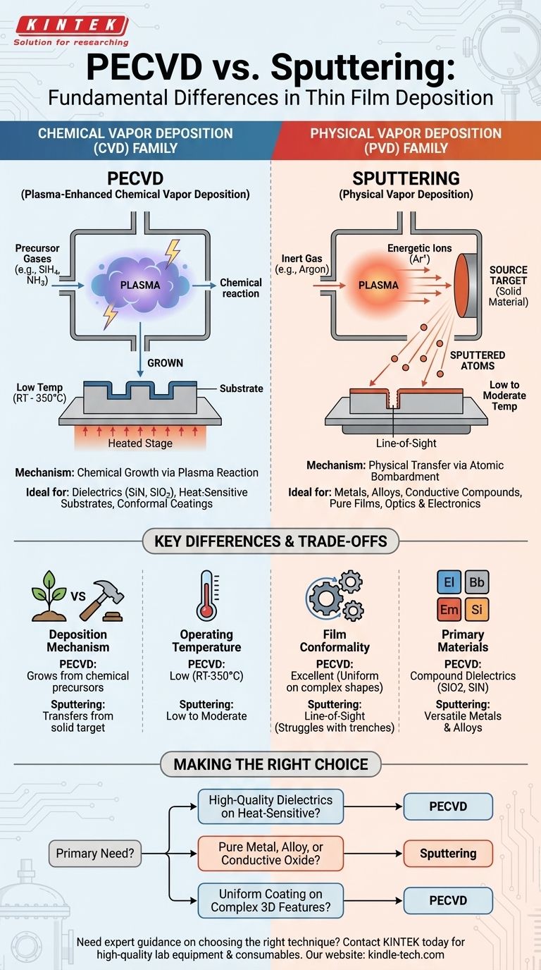
At their core, PECVD and sputtering are fundamentally different methods for creating a thin film. Sputtering is a physical process that uses energetic ions to physically knock atoms from a source target onto a substrate. In contrast, Plasma-Enhanced Chemical Vapor Deposition (PECVD) is a chemical process that uses plasma to drive chemical reactions from precursor gases, allowing a new material to "grow" on the substrate surface at low temperatures.
The most critical distinction is how the film material arrives at the substrate. Sputtering is a physical transfer—like a nanoscale sandblaster—while PECVD is a chemical reaction—like precisely controlled condensation. This single difference dictates the materials you can use, the properties of the final film, and the substrates you can coat.
The Fundamental Divide: Chemical vs. Physical Deposition
To understand the difference between these two techniques, you must first recognize that they belong to two separate families of thin-film deposition: Chemical Vapor Deposition (CVD) and Physical Vapor Deposition (PVD).
Chemical Vapor Deposition (CVD) Explained
In a traditional CVD process, precursor gases are introduced into a chamber and heated to very high temperatures (often 600–800°C). This thermal energy breaks the chemical bonds in the gases, initiating a reaction that deposits a solid film onto the substrate.
How PECVD Refines the Process
PECVD is a modern variant of CVD designed to overcome the high-temperature requirement. Instead of relying solely on heat, it introduces an energy-rich plasma into the chamber.
This plasma provides the necessary energy to break down the precursor gases and drive the chemical reaction, allowing for high-quality film deposition at much lower temperatures (typically room temperature to 350°C). This makes it indispensable for coating heat-sensitive materials, such as integrated circuits in their final manufacturing stages.
Physical Vapor Deposition (PVD) Explained
PVD techniques do not involve chemical reactions. Instead, they work by physically moving material from a solid source (called a "target") to the substrate in a vacuum. This can be done by heating the source until it evaporates or, in the case of sputtering, by bombarding it with ions.
How Sputtering Works
Sputtering is a highly controlled PVD process. It begins by introducing an inert gas, typically Argon, into a vacuum chamber and creating a plasma. The positively charged Argon ions are then accelerated by an electric field and directed at the target.
When these ions collide with the target, they physically knock off, or "sputter," atoms of the target material. These ejected atoms then travel through the vacuum and deposit onto the substrate, building up the thin film atom by atom.
Key Differences in Application and Outcome
The mechanical and chemical differences between PECVD and sputtering lead to significant variations in their use and the resulting films.
Deposition Mechanism: Growing vs. Bombarding
PECVD grows a film from chemical precursors. This means the resulting material (e.g., silicon nitride) can be different from the starting gases (e.g., silane and ammonia).
Sputtering transfers a film via atomic bombardment. The film is composed of the same material as the target, making it ideal for depositing pure metals, alloys, and specific compounds with high fidelity.
Operating Temperature
This is a critical differentiator. PECVD is a low-temperature process by design, making it perfect for substrates that cannot withstand the high heat of traditional CVD. While sputtering is also considered a low-temperature process, PECVD was specifically developed to deposit materials like high-quality dielectrics onto finished electronic components without damaging them.
Film Properties and Quality
PECVD is renowned for producing dense, pinhole-free, and conformal films. Because the deposition is driven by a chemical reaction that can occur on all exposed surfaces, it is excellent at uniformly coating complex shapes with high "step coverage."
Sputtering deposits material in a "line-of-sight" fashion. While it produces very dense films with excellent adhesion, it can struggle to uniformly coat intricate topographies with deep trenches or sharp corners.
Material Versatility
Sputtering is exceptionally versatile for depositing a vast range of materials, including nearly any metal, alloy, or electrically conductive compound. If you have a solid target of the material, you can likely sputter it.
PECVD is specialized for depositing compound materials, particularly dielectrics like silicon dioxide (SiO2) and silicon nitride (SiN), which are critical for insulating layers in the semiconductor industry.
Understanding the Trade-offs
Neither method is universally superior; the choice depends entirely on the goal.
The Challenge of Conformal Coatings
Sputtering's line-of-sight nature is a limitation for 3D structures. The top surfaces receive more material than the sidewalls, a phenomenon known as shadowing. PECVD's chemical nature gives it a distinct advantage here, providing much more uniform coverage over complex features.
Managing Film Stress
The energetic ion bombardment in sputtering can induce significant compressive stress in the deposited film. While this often improves density, excessive stress can cause the film to crack or delaminate. PECVD film stress is controlled by different parameters (plasma power, gas flow) and must also be carefully managed.
Complexity and Contamination
Because PECVD uses reactive gases, byproducts can be incorporated into the film. For instance, hydrogen from precursor gases is often present in PECVD films, which can affect optical or electrical properties. Sputtering, using an inert gas, can produce films of extremely high purity, limited only by the purity of the target material itself.
Making the Right Choice for Your Application
Your decision should be guided by your material needs, substrate limitations, and the geometry of the part you are coating.
- If your primary focus is depositing high-quality dielectrics (SiO2, SiN) on a temperature-sensitive substrate: PECVD is the clear choice due to its low-temperature operation and excellent film quality.
- If your primary focus is depositing a pure metal, complex alloy, or conductive oxide for optics or electronics: Sputtering offers unmatched material versatility, purity, and control.
- If your primary focus is achieving a uniform coating on a component with complex 3D features: PECVD generally provides superior conformality and step coverage compared to line-of-sight sputtering.
Ultimately, choosing the right technique requires a clear understanding of your end goal and the trade-offs between a chemical growth process and a physical transfer process.
Summary Table:
| Feature | PECVD (Plasma-Enhanced Chemical Vapor Deposition) | Sputtering (Physical Vapor Deposition) |
|---|---|---|
| Core Mechanism | Chemical reaction (film growth) | Physical transfer (atomic bombardment) |
| Operating Temperature | Low (Room Temp - 350°C) | Low (Room Temp - Moderate) |
| Film Conformality | Excellent (uniform on complex shapes) | Line-of-sight (can struggle with trenches) |
| Primary Materials | Dielectrics (e.g., SiN, SiO2) | Metals, Alloys, Conductive Compounds |
| Ideal For | Heat-sensitive substrates, ICs, conformal coatings | Pure materials, optics, electronics, high-purity films |
Need expert guidance on choosing the right deposition technique for your application?
At KINTEK, we specialize in providing high-quality lab equipment and consumables for all your thin-film deposition needs. Whether you require the low-temperature, conformal capabilities of PECVD or the material versatility and purity of sputtering, our experts can help you select the perfect solution for your laboratory.
Contact us today to discuss your specific requirements and discover how KINTEK can enhance your research and production processes.
Visual Guide
Related Products
- Inclined Rotary Plasma Enhanced Chemical Vapor Deposition PECVD Equipment Tube Furnace Machine
- Chemical Vapor Deposition CVD Equipment System Chamber Slide PECVD Tube Furnace with Liquid Gasifier PECVD Machine
- Inclined Rotary Plasma Enhanced Chemical Vapor Deposition PECVD Equipment Tube Furnace Machine
- RF PECVD System Radio Frequency Plasma-Enhanced Chemical Vapor Deposition RF PECVD
- Multi Heating Zones CVD Tube Furnace Machine Chemical Vapor Deposition Chamber System Equipment
People Also Ask
- What are the advantages of plasma enhanced chemical vapor deposition? Enable Low-Temperature, High-Quality Film Deposition
- Why is a PECVD system required for vertical graphene synthesis? Master Directional Control for 3D Nanostructures
- How does plasma enhanced chemical vapor deposition work? Enable Low-Temperature Thin Film Deposition
- What are the core advantages of PE-CVD in OLED encapsulation? Protect Sensitive Layers with Low-Temp Film Deposition
- What are the benefits of plasma enhanced CVD? Achieve High-Quality, Low-Temperature Film Deposition


