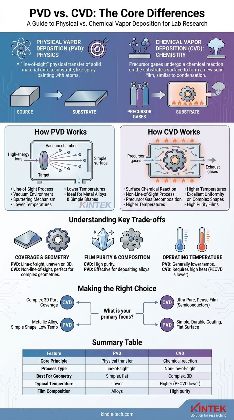
At its core, the difference is a matter of physics versus chemistry. Physical Vapor Deposition (PVD) is a "line-of-sight" process that physically transfers a solid material onto a substrate, much like spray painting with atoms. In contrast, Chemical Vapor Deposition (CVD) uses precursor gases that undergo a chemical reaction on the substrate's surface to form a new, solid film, similar to how dew condenses on a cold surface.
The fundamental distinction is how the coating material arrives at the surface. PVD physically transports atoms in a straight line from a source to the target, while CVD uses a chemical gas to coat all exposed surfaces uniformly through a chemical reaction.
How Physical Vapor Deposition (PVD) Works
The Core Principle: A "Line-of-Sight" Process
PVD is a mechanical coating process performed in a vacuum. It relies on a direct, unobstructed path between the material source and the substrate being coated.
This means that only the surfaces that can be "seen" by the source material will receive the coating.
The Mechanism of Transfer
In common PVD methods like sputtering, a solid block of the coating material (the "target") is bombarded with high-energy ions. This impact physically dislodges or "sputters" atoms from the target.
These dislodged atoms then travel in a straight line through the vacuum chamber, eventually striking the substrate and building up as a thin film.
Key Characteristics of PVD
Because of its physical nature, PVD is often performed at relatively low temperatures. It is exceptionally well-suited for depositing metal alloys and coating simpler, flatter substrate geometries where uniform coverage of complex shapes is not a requirement.
How Chemical Vapor Deposition (CVD) Works
The Core Principle: A Surface Chemical Reaction
CVD is a chemical process that relies on the decomposition of reactive gases to create a film. The coating is not transferred from a solid source but is created directly on the substrate.
The Mechanism of Formation
One or more volatile precursor gases are introduced into a reaction chamber containing the heated substrate. The heat provides the energy needed to initiate a chemical reaction on and near the substrate's surface.
This reaction breaks down the precursor gases, depositing a solid material film onto the substrate and creating volatile byproducts that are then exhausted from the chamber.
Key Characteristics of CVD
CVD is a non-line-of-sight process. The precursor gases surround the substrate, allowing the chemical reaction to occur evenly on all surfaces. This makes it ideal for uniformly coating components with complex shapes.
The process offers exceptional control, capable of creating ultra-pure, dense, and extremely thin layers, which is why it is critical in the manufacturing of electrical circuits and semiconductors.
Understanding the Key Trade-offs
Coverage and Geometry
This is the most significant difference. PVD's line-of-sight nature makes it perfect for coating flat surfaces but results in uneven coverage on complex 3D parts.
CVD excels at creating a perfectly uniform (or "conformal") coating over intricate and complex geometries because the gas can reach every surface.
Film Purity and Composition
CVD can produce films of extremely high purity because the precursor gases can be refined to exacting standards.
PVD is highly effective for depositing alloys, as the composition of the source target is directly transferred to the substrate.
Operating Temperature
PVD methods generally operate at lower temperatures than traditional CVD processes.
Standard CVD requires high heat to drive the necessary chemical reactions, though specialized methods like Plasma-Enhanced CVD (PECVD) use plasma to enable these reactions at lower temperatures.
Making the Right Choice for Your Application
Your final decision must be guided by the specific requirements of your component's geometry, the desired material properties, and your process temperature constraints.
- If your primary focus is uniformly coating a complex, 3D part: CVD is the clear choice due to its non-line-of-sight chemical reaction process.
- If your primary focus is depositing a metallic alloy onto a simple shape at low temperatures: PVD is often the more direct and efficient method.
- If your primary focus is creating an ultra-pure, dense film for a semiconductor application: CVD is the industry standard, offering unparalleled control and purity.
- If your primary focus is a simple, durable coating on a relatively flat surface: PVD provides a robust and well-established solution.
Ultimately, choosing the right method requires matching the distinct physical or chemical nature of the process to the desired outcome for your product.
Summary Table:
| Feature | PVD (Physical Vapor Deposition) | CVD (Chemical Vapor Deposition) |
|---|---|---|
| Core Principle | Physical transfer of atoms | Chemical reaction on the surface |
| Process Type | Line-of-sight | Non-line-of-sight |
| Best For Geometry | Simpler, flatter surfaces | Complex, 3D parts |
| Typical Temperature | Lower temperatures | Higher temperatures (PECVD is lower) |
| Film Composition | Excellent for metal alloys | Exceptional purity and control |
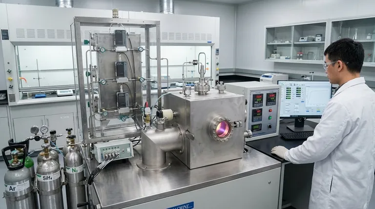
Need expert guidance on selecting the right deposition process for your lab?
The choice between PVD and CVD is critical for achieving the desired film properties, coverage, and performance on your substrates. KINTEK specializes in providing high-quality lab equipment and consumables for all your vapor deposition needs. Our experts can help you navigate these technical decisions to optimize your research and production outcomes.
Contact us today via our [#ContactForm] to discuss how our solutions can enhance your laboratory's capabilities and efficiency.
Visual Guide
Related Products
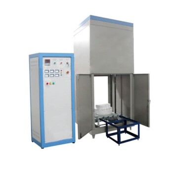
- Inclined Rotary Plasma Enhanced Chemical Vapor Deposition PECVD Equipment Tube Furnace Machine
- HFCVD Machine System Equipment for Drawing Die Nano-Diamond Coating
- 915MHz MPCVD Diamond Machine Microwave Plasma Chemical Vapor Deposition System Reactor
- Vacuum Hot Press Furnace Machine for Lamination and Heating
- 1200℃ Split Tube Furnace with Quartz Tube Laboratory Tubular Furnace
People Also Ask
- What is the difference between PECVD and CVD? Unlock the Right Thin-Film Deposition Method
- What materials are deposited in PECVD? Discover the Versatile Thin-Film Materials for Your Application
- What is PECVD silicon deposition? Achieve Low-Temperature, High-Quality Thin Films
- What is PECVD used for? Achieve Low-Temperature, High-Performance Thin Films
- What is meant by vapor deposition? A Guide to Atomic-Level Coating Technology