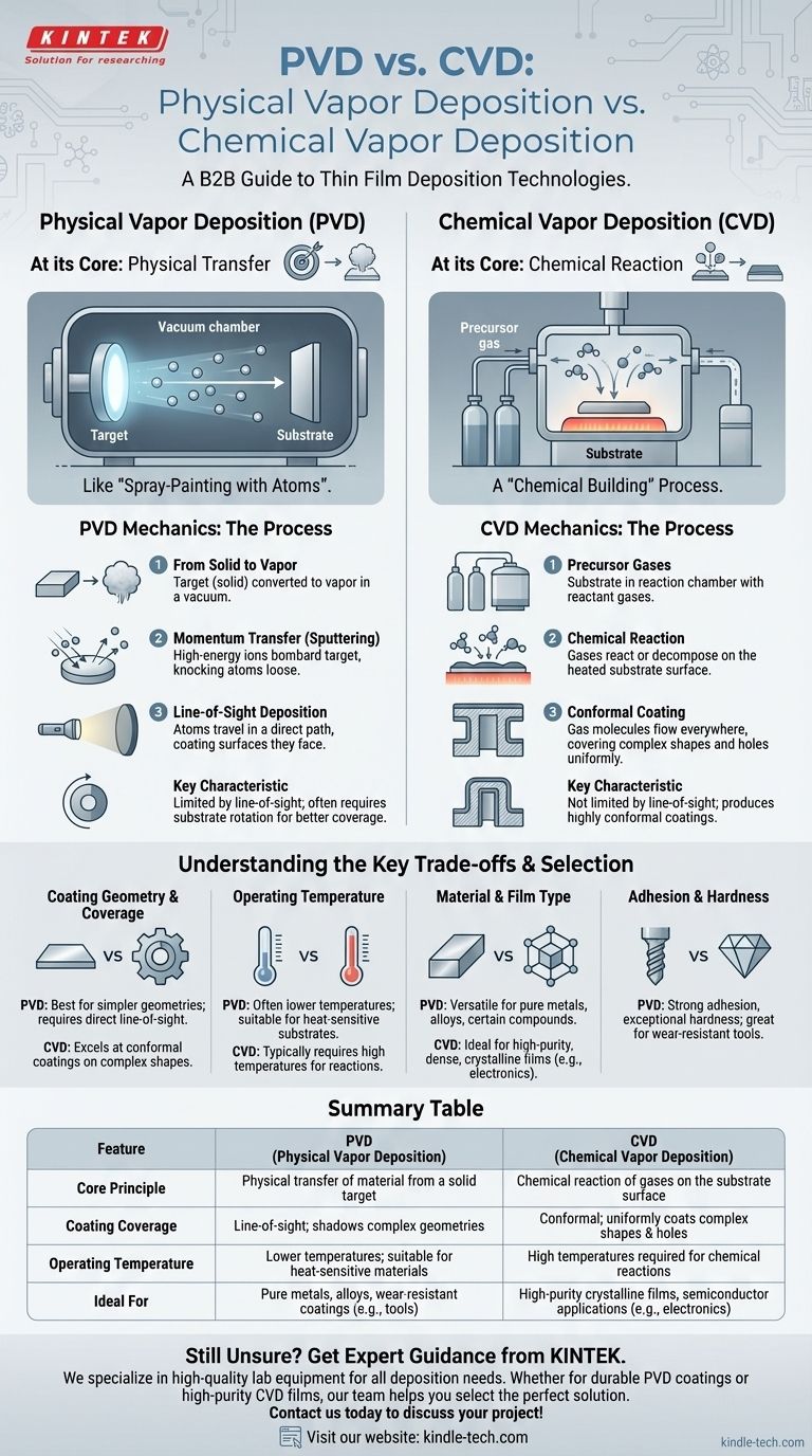
At its core, the difference is physical versus chemical. Physical Vapor Deposition (PVD) physically transfers a coating material from a solid source onto a substrate, much like spray-painting with individual atoms. In contrast, Chemical Vapor Deposition (CVD) uses precursor gases that chemically react on the substrate's surface to grow an entirely new solid film from the ground up.
Think of PVD as a "line-of-sight" physical transfer process, where atoms are knocked off a target and stick to a surface. CVD is a chemical building process, where gas molecules cover all surfaces and react to form a new, highly uniform layer. This distinction dictates which method is suitable for a given material, geometry, and application.
The Mechanics of Physical Vapor Deposition (PVD)
The Core Principle: A Physical Transfer
PVD is a process where a solid material, known as the "target," is converted into a vapor within a vacuum chamber.
This vapor then travels and condenses onto the object (the "substrate") to form the thin film coating. The coating material itself does not undergo a chemical change.
From Solid to Vapor
The most common PVD method is sputtering, where the target is bombarded with high-energy ions (typically from a gas like argon).
This bombardment physically knocks atoms loose from the target through momentum transfer, launching them toward the substrate without ever melting the source material.
The "Line-of-Sight" Characteristic
PVD is fundamentally a line-of-sight process.
This means the coating material only deposits on surfaces that have a direct, unobstructed path from the source, similar to how a flashlight casts a shadow. Objects are often rotated to ensure more complete coverage.
The Mechanics of Chemical Vapor Deposition (CVD)
The Core Principle: A Chemical Reaction
CVD does not simply transfer an existing material; it creates a new one directly on the substrate's surface.
This is achieved through a controlled chemical reaction, which forms a solid film from gaseous reactants.
Using Precursor Gases
The substrate is placed inside a reaction chamber filled with one or more volatile precursor gases.
When these gases come into contact with the heated substrate, they react or decompose, leaving behind a solid material that builds up layer by layer.
The Advantage of Conformal Coating
Because the gas molecules can flow and reach all exposed areas, CVD is not limited by line-of-sight.
It produces a highly conformal coating, meaning it uniformly covers complex shapes, sharp corners, and even the inside of holes with consistent thickness.
Understanding the Key Trade-offs
Coating Geometry and Coverage
PVD is best suited for coating simpler geometries or flat surfaces where direct line-of-sight is achievable.
CVD excels at providing uniform coatings on intricate parts with complex topographies that PVD cannot reach evenly.
Operating Temperature
PVD processes can often be performed at lower temperatures, making them suitable for substrates that cannot withstand high heat.
CVD typically requires very high temperatures to activate the necessary chemical reactions, which can limit the types of materials that can be coated without being damaged.
Material and Film Type
PVD is highly versatile for depositing pure metals, alloys, and certain compounds directly from a solid target.
CVD is the dominant method for creating extremely pure, dense, and often crystalline films, making it essential in the semiconductor and electronics industries.
Adhesion and Hardness
PVD coatings, particularly from ionized processes like arc deposition, are known for their strong adhesion and exceptional hardness. This makes PVD a go-to choice for creating durable, wear-resistant surfaces on tools.
Making the Right Choice for Your Application
Selecting the correct process requires aligning the method's strengths with your primary objective.
- If your primary focus is coating a complex part with uniform thickness: CVD is the superior choice due to its non-line-of-sight, conformal nature.
- If your primary focus is depositing a pure metal or alloy onto a temperature-sensitive substrate: PVD is generally more suitable because it can operate at lower temperatures.
- If your primary focus is creating an extremely hard, wear-resistant surface on a cutting tool: PVD methods like sputtering provide the necessary durability and strong adhesion.
- If your primary focus is growing a high-purity crystalline film for electronics: CVD is the established industry standard for this level of precision and material quality.
Understanding this fundamental difference between physical transfer and chemical creation is the key to selecting the right technology for your specific engineering goal.
Summary Table:
| Feature | PVD (Physical Vapor Deposition) | CVD (Chemical Vapor Deposition) |
|---|---|---|
| Core Principle | Physical transfer of material from a solid target | Chemical reaction of gases on the substrate surface |
| Coating Coverage | Line-of-sight; shadows complex geometries | Conformal; uniformly coats complex shapes & holes |
| Operating Temperature | Lower temperatures; suitable for heat-sensitive materials | High temperatures required for chemical reactions |
| Ideal For | Pure metals, alloys, wear-resistant coatings | High-purity crystalline films, semiconductor applications |
Still unsure whether PVD or CVD is right for your lab's specific needs?
At KINTEK, we specialize in providing expert guidance and high-quality lab equipment for all your deposition requirements. Whether you need durable PVD coatings for tools or high-purity CVD films for electronics, our team can help you select the perfect solution.
Contact us today via our [#ContactForm] to discuss your project and discover how KINTEK's expertise in lab equipment and consumables can enhance your research and production processes.
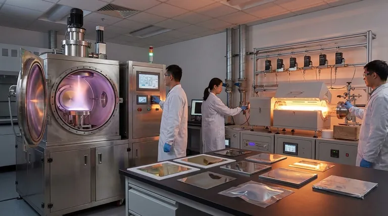
Visual Guide
Related Products
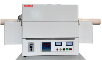
- Chemical Vapor Deposition CVD Equipment System Chamber Slide PECVD Tube Furnace with Liquid Gasifier PECVD Machine
- Inclined Rotary Plasma Enhanced Chemical Vapor Deposition PECVD Equipment Tube Furnace Machine
- RF PECVD System Radio Frequency Plasma-Enhanced Chemical Vapor Deposition RF PECVD
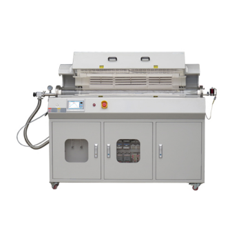
- Customer Made Versatile CVD Tube Furnace Chemical Vapor Deposition Chamber System Equipment
- Vacuum Hot Press Furnace Machine for Lamination and Heating
People Also Ask
- What is the precursor gas in PECVD? The Key to Low-Temperature Thin Film Deposition
- How are PECVD and CVD different? A Guide to Choosing the Right Thin-Film Deposition Process
- How plasma is generated in PECVD? A Step-by-Step Breakdown of the Process
- What is the difference between thermal CVD and PECVD? Choose the Right Thin-Film Deposition Method
- How is PECVD different from CVD? Unlock Low-Temperature Thin Film Deposition