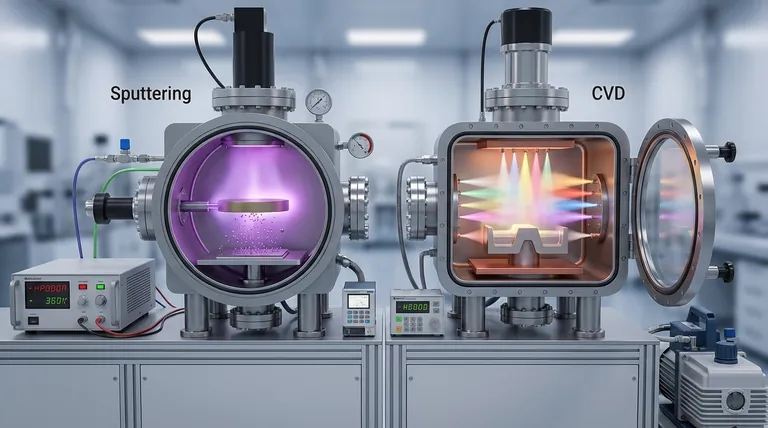
At a fundamental level, the difference between sputtering and CVD is a matter of physics versus chemistry. Sputtering is a Physical Vapor Deposition (PVD) method that physically knocks atoms off a solid target using ion bombardment, like a sandblaster at the atomic scale. In contrast, Chemical Vapor Deposition (CVD) is a chemical process that uses precursor gases that react and decompose on a heated surface to build the desired film.
The choice between sputtering and CVD hinges on this core distinction: Sputtering physically transfers material from a solid source, offering immense material flexibility. CVD chemically constructs the film from gaseous precursors, excelling at creating highly pure and uniform coatings on complex shapes.
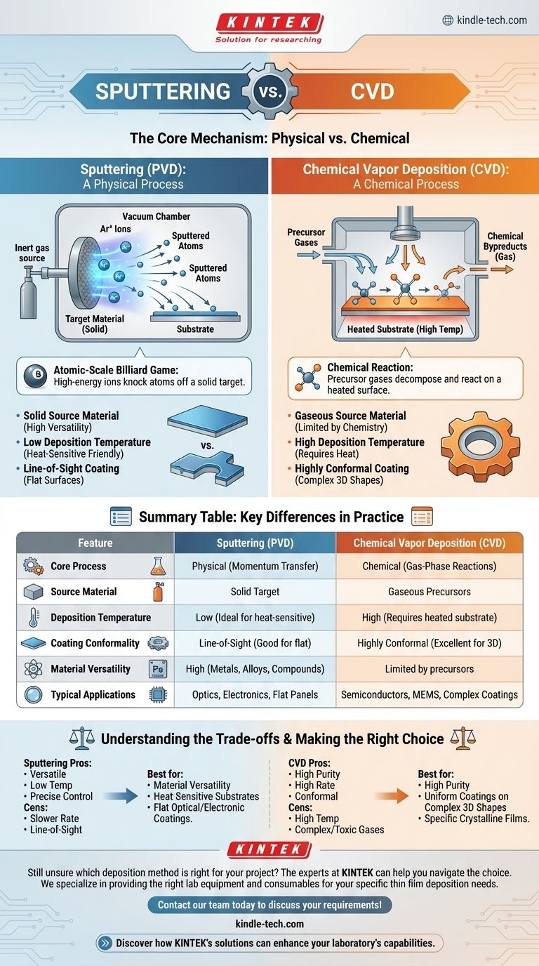
The Core Mechanism: Physical vs. Chemical
To select the right technique, you must first understand how each process operates at a molecular level. Their names—Physical Vapor Deposition versus Chemical Vapor Deposition—are a direct description of their fundamental nature.
How Sputtering Works: A Physical Process
Sputtering is a sub-category of PVD. Think of it as an atomic-scale billiard game.
In a high-vacuum chamber, a high voltage is used to create a plasma from an inert gas, typically argon. These positively charged argon ions are accelerated and slammed into a solid plate of the material you wish to deposit, known as the target.
This high-energy impact physically ejects or "sputters" atoms from the target. These dislodged atoms then travel through the vacuum and deposit onto your component (the substrate), gradually building a thin film.
How CVD Works: A Chemical Process
CVD does not begin with a solid block of material. Instead, it relies entirely on chemical reactions.
Volatile precursor gases, which contain the elements required for the film, are introduced into a reaction chamber.
The substrate is heated to a high temperature, providing the energy needed to trigger a chemical reaction. The precursor gases decompose on the hot substrate surface, bonding to it and releasing their desired elements to form the film.
Unwanted chemical byproducts from this reaction are simply pumped out of the chamber as gas.
Key Differences in Practice
The physical and chemical mechanisms of these processes lead to critical differences in their practical application, from material choice to the shape of the parts you can coat.
The Source Material
Sputtering uses a solid target. This provides incredible versatility, as almost any metal, alloy, or compound that can be formed into a solid plate can be used as a source material.
CVD is limited to materials that can be delivered in a stable, volatile precursor gas. This requires specialized chemistry and restricts the available palette of materials compared to sputtering.
Deposition Temperature
CVD generally requires very high substrate temperatures (often several hundred degrees Celsius) to drive the necessary chemical reactions. This can prevent its use on temperature-sensitive materials like plastics or certain alloys.
Sputtering is a much lower-temperature process. Since it's a physical transfer of momentum, high heat isn't required, making it ideal for coating heat-sensitive substrates.
Film Quality and Conformance
Sputtering is a line-of-sight technique. The sputtered atoms travel in a relatively straight line from the target to the substrate. This makes it excellent for coating flat surfaces but poor at coating complex, 3D shapes uniformly.
CVD excels at creating highly conformal coatings. Because the precursor is a gas, it flows around and into every feature of a complex part, resulting in a perfectly uniform film thickness over even the most intricate geometries.
Understanding the Trade-offs and Limitations
Neither method is universally superior. The optimal choice depends on balancing the inherent trade-offs of each process against your specific goals.
Material Purity and Contamination
CVD can produce films of exceptionally high purity, as the process can be fine-tuned to deposit only the desired material. However, precursors can sometimes leave behind contaminants like carbon or hydrogen if the reaction is incomplete.
Sputtering is a very clean process, but it's possible for atoms from the sputtering gas (e.g., argon) to become embedded in the growing film as an impurity.
Deposition Rate and Control
Sputtering deposition rates are typically slower but offer very stable and precise control over film thickness and composition, which is critical for applications like optical coatings.
CVD can often achieve much higher deposition rates. However, managing the complex gas-phase chemistry to ensure uniformity and prevent unwanted particle formation can be more challenging.
System Complexity and Cost
Sputtering systems, while requiring high-vacuum technology, are generally more straightforward in their operation and material handling.
CVD systems can be more complex and expensive, especially when they require very high temperatures or involve the handling of toxic, corrosive, or pyrophoric precursor gases.
Making the Right Choice for Your Application
Your decision should be driven by the non-negotiable requirements of your final product.
- If your primary focus is material versatility and coating heat-sensitive substrates: Sputtering is the superior choice due to its use of solid targets and lower processing temperatures.
- If your primary focus is creating highly pure, uniform coatings on complex 3D shapes: CVD is the definitive method, as its chemical gas-phase nature allows for unmatched conformality.
- If your primary focus is depositing a wide range of metals or simple dielectrics on flat substrates: Sputtering provides a reliable, well-controlled, and cost-effective solution for applications like optics and electronics.
- If your primary focus is growing specific crystalline or compound films like silicon dioxide or tungsten carbide: CVD is often the only option, as these films are constructed through specific chemical reactions.
Understanding this core physical-versus-chemical distinction empowers you to select the deposition technique that best aligns with your material, geometry, and performance goals.
Summary Table:
| Feature | Sputtering (PVD) | Chemical Vapor Deposition (CVD) |
|---|---|---|
| Core Process | Physical (momentum transfer) | Chemical (gas-phase reactions) |
| Source Material | Solid target | Gaseous precursors |
| Deposition Temperature | Low (ideal for heat-sensitive substrates) | High (requires heated substrate) |
| Coating Conformality | Line-of-sight (good for flat surfaces) | Highly conformal (excellent for complex 3D shapes) |
| Material Versatility | High (metals, alloys, compounds) | Limited by available precursor gases |
| Typical Applications | Optics, electronics, flat panel displays | Semiconductors, MEMS, complex geometry coatings |
Still unsure which deposition method is right for your project? The experts at KINTEK can help you navigate the choice between sputtering and CVD. We specialize in providing the right lab equipment and consumables for your specific thin film deposition needs.
Contact our team today to discuss your application requirements and discover how KINTEK's solutions can enhance your laboratory's capabilities and efficiency.
Visual Guide
Related Products
- Split Chamber CVD Tube Furnace with Vacuum Station Chemical Vapor Deposition System Equipment Machine
- Chemical Vapor Deposition CVD Equipment System Chamber Slide PECVD Tube Furnace with Liquid Gasifier PECVD Machine
- Customer Made Versatile CVD Tube Furnace Chemical Vapor Deposition Chamber System Equipment
- CVD Diamond for Thermal Management Applications
- RF PECVD System Radio Frequency Plasma-Enhanced Chemical Vapor Deposition RF PECVD
People Also Ask
- What temperature is maintained in CVD? Unlocking the High-Heat Process for Superior Coatings
- How does a tube CVD reactor facilitate N-CNT growth? Master Precision Synthesis on Carbon Paper
- What is a split tube furnace? Unlock Unmatched Access for Complex Lab Setups
- What is the function of a high-temperature CVD tube furnace in 3D graphene foam prep? Master 3D Nanomaterial Growth
- What is the function of a tube furnace in CVD SiC synthesis? Achieving Ultra-Pure Silicon Carbide Powders


