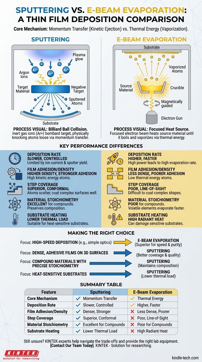
At a fundamental level, the difference between sputtering and e-beam evaporation lies in how atoms are liberated from a source material. Sputter deposition uses momentum transfer, where energetic gas ions bombard a target to physically knock atoms loose. In contrast, electron beam (e-beam) evaporation uses thermal energy, where a focused beam of electrons heats a material until it boils and vaporizes.
While both are methods of physical vapor deposition (PVD) used to create thin films, the choice between them is not about which is "better." It's about which mechanism—kinetic bombardment versus thermal vaporization—best suits the specific material, substrate, and desired film properties for your application.
The Core Mechanism: Momentum vs. Heat
To understand the practical outcomes of each technique, you must first grasp their distinct physical processes. One is a mechanical collision, and the other is a phase change from solid to gas.
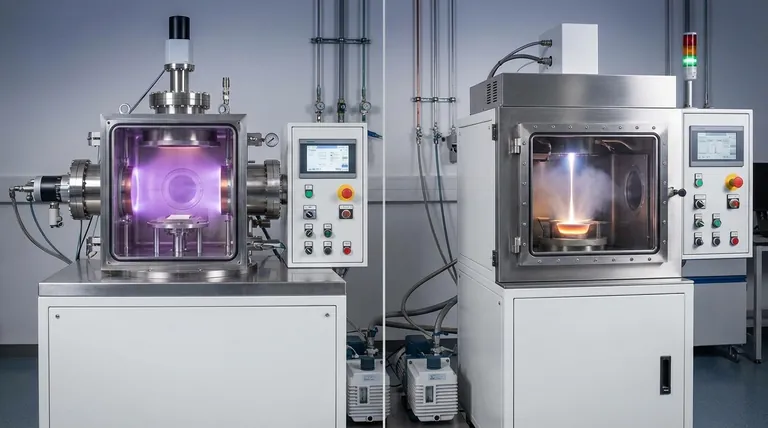
How Sputtering Works: A Billiard Ball Collision
In sputtering, the deposition chamber is filled with an inert gas, typically Argon. A high voltage is applied, creating a plasma of positively charged Argon ions.
These ions are accelerated into a negatively charged source material, called the target. When the ions collide with the target, they transfer their kinetic energy and eject, or "sputter," atoms from the target's surface.
These ejected atoms travel through the chamber and land on your substrate, gradually building up a thin film. This process is more akin to a microscopic sandblasting than it is to evaporation.
How E-Beam Evaporation Works: A Focused Heat Source
E-beam evaporation takes place in a high vacuum. A high-intensity beam of electrons is generated and magnetically guided to strike a source material held in a crucible.
The immense energy from the electron beam rapidly heats the source material, causing it to melt and then evaporate (or sublimate).
This creates a vapor cloud of atoms that rises from the source, travels in a straight line-of-sight path, and condenses on the cooler substrate, forming the thin film.
Key Performance Differences Explained
The fundamental difference between kinetic ejection and thermal evaporation leads to significant variations in film quality, deposition speed, and application suitability.
Deposition Rate: Speed vs. Control
E-beam evaporation generally has a much higher deposition rate than sputtering. The ability to increase electron beam power directly translates to a higher evaporation rate, making it very efficient for thick films.
Sputtering is a slower, more controlled process. The deposition rate is limited by factors like ion current density and the sputter yield of the target material. This is particularly true for dielectric (insulating) materials, which are notoriously slow to sputter.
Film Adhesion and Density: High vs. Low Energy
Sputtered atoms are knocked from the target with significant kinetic energy (tens of electron-volts). When they strike the substrate, this energy helps them form a denser, more strongly adhered film.
Evaporated atoms, by contrast, leave the source with only low thermal energy (tenths of an electron-volt). This can result in films that are less dense and may have poorer adhesion unless the substrate is heated.
Step Coverage: Coating Complex Surfaces
Sputtering offers superior step coverage. Because the process operates at a higher pressure, sputtered atoms are scattered by the gas on their way to the substrate. This allows them to coat the sidewalls and complex topographical features of a substrate more conformally.
E-beam evaporation is a line-of-sight process. The vaporized atoms travel in a straight line from the source to the substrate. This makes it difficult to coat vertical sidewalls or the interior of trenches, resulting in poor coverage on non-flat surfaces.
Understanding the Trade-offs
Choosing a deposition method involves weighing the advantages against their inherent limitations. Neither technique is a universal solution.
Substrate Heating and Damage
The intense radiant heat from the molten source in e-beam evaporation can significantly heat the substrate. This can damage temperature-sensitive materials like plastics or certain semiconductor devices.
Sputtering is a "colder" process in terms of thermal load, making it suitable for heat-sensitive substrates. However, the bombardment of the substrate by energetic particles can sometimes cause structural damage or stress in the growing film.
Material Purity and Composition
E-beam evaporation, conducted in a high vacuum, can produce extremely pure films for single-element materials. However, it struggles with alloys or compounds where elements have different vapor pressures, as the more volatile element will evaporate faster, changing the film's composition.
Sputtering is excellent at preserving the stoichiometry of compound materials. The kinetic ejection process transfers the material from target to substrate without significantly altering its elemental ratios. The primary impurity risk comes from the potential incorporation of the process gas (e.g., Argon) into the film.
Scalability and Automation
Sputtering systems, particularly magnetron sputtering, are highly scalable and well-suited for automation. They are widely used for coating very large areas, such as architectural glass or flat-panel displays.
While e-beam can be used for large-scale production (e.g., solar panels), achieving high uniformity over very large, complex areas can be more challenging.
Making the Right Choice for Your Application
Your decision must be driven by the specific requirements of the thin film you intend to create. Consider the following guidelines based on your primary goal.
- If your primary focus is high-speed deposition for simple optics or metal layers: E-beam evaporation is often the superior choice due to its high rates and material purity.
- If your primary focus is creating dense, adhesive films on complex 3D substrates: Sputtering provides better coverage and film quality for challenging topographies.
- If your primary focus is depositing compound materials or alloys with precise stoichiometry: Sputtering generally maintains the original material composition more reliably.
- If your primary focus is coating temperature-sensitive substrates: Sputtering's lower thermal load makes it a safer option than e-beam evaporation.
Ultimately, selecting the correct deposition technique is a critical engineering decision that directly impacts the performance and reliability of your final product.
Summary Table:
| Feature | Sputtering | E-Beam Evaporation |
|---|---|---|
| Core Mechanism | Momentum transfer (kinetic ejection) | Thermal energy (vaporization) |
| Deposition Rate | Slower, more controlled | Higher, faster |
| Film Adhesion/Density | Denser, stronger adhesion | Less dense, may have poorer adhesion |
| Step Coverage | Superior, conformal coating | Poor, line-of-sight only |
| Material Stoichiometry | Excellent for compounds/alloys | Poor for compounds/alloys |
| Substrate Heating | Lower thermal load, 'colder' process | High radiant heat, can damage substrates |
Still unsure which PVD method is right for your application? The experts at KINTEK can help you navigate the trade-offs between sputtering and e-beam evaporation. We specialize in providing the right lab equipment and consumables to meet your specific thin film deposition challenges, ensuring optimal film quality and process efficiency. Contact our team today for a personalized consultation and discover how KINTEK can support your laboratory's success.
Visual Guide
Related Products
- Spark Plasma Sintering Furnace SPS Furnace
- Vacuum Induction Melting Spinning System Arc Melting Furnace
- Chemical Vapor Deposition CVD Equipment System Chamber Slide PECVD Tube Furnace with Liquid Gasifier PECVD Machine
- Customer Made Versatile CVD Tube Furnace Chemical Vapor Deposition Chamber System Equipment
People Also Ask
- What are the advantages of CAMI/SPS for W-Cu composite preparation? Reduce cycles from hours to seconds.
- What are the fundamentals of spark plasma sintering process? Unlock Rapid, High-Performance Material Consolidation
- What is the theory of spark plasma sintering? A Guide to Rapid, Low-Temperature Densification
- What technical advantages does a Spark Plasma Sintering (SPS) furnace offer for LZP ceramics? Enhance Ionic Conductivity
- What is the process fundamentals of spark plasma sintering? Achieve Rapid, High-Density Material Consolidation


