The primary difference between sputtering and ion beam deposition lies in the location and control of the plasma. In standard magnetron sputtering, the material to be coated (the substrate) is immersed in the same plasma that generates the ions to strike the source material. In ion beam deposition, a separate ion source creates a focused beam that strikes the source material, and this entire process occurs away from the substrate, which remains outside the plasma environment.
At its core, the choice between these two methods is a choice between process integration and process separation. Standard sputtering is a direct, brute-force method where everything happens in one plasma chamber, while ion beam deposition is an indirect, high-precision technique that decouples ion generation from material deposition.
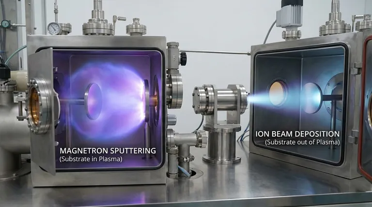
The Fundamental Separation: Plasma vs. Ion Beam
Both techniques are forms of Physical Vapor Deposition (PVD), a category of processes where a material is converted into a vapor phase and then condensed onto a substrate to form a thin film. The key difference is how that vapor is created.
How Standard Sputtering Works
In a typical magnetron sputtering system, an inert gas like argon is introduced into a vacuum chamber.
A strong electric and magnetic field is applied, which ignites the gas into a plasma, a high-energy state of ions and electrons.
These ions are accelerated into a source material, known as the target. The impact physically knocks off, or "sputters," atoms from the target, which then travel and coat the nearby substrate. The substrate is inside this plasma environment.
How Ion Beam Deposition Works
Ion beam deposition adds a critical layer of separation and control to this process.
An independent ion source generates a highly controlled, focused beam of ions completely separate from the target and the substrate.
This beam is then directed at the target in a different part of the chamber, sputtering atoms just like in the standard process. However, because the substrate is not in the plasma, it is not bombarded by high-energy particles.
Key Advantages of Ion Beam Deposition
This separation of the ion source from the substrate creates several distinct advantages, making it the preferred method for high-performance applications.
Independent Control Over Film Properties
Because the ion beam's energy and current are controlled independently, operators can precisely tune the properties of the deposited film.
This can increase film density, modify the crystalline structure, and improve characteristics like water permeability, leading to superior performance.
Reduced Contamination
In standard sputtering, the inert gas from the plasma can become embedded in the growing film, which can be a source of contamination.
Ion beam deposition significantly reduces this sputter gas inclusion because the substrate is isolated from the main plasma environment, resulting in purer thin films.
Protection for Sensitive Substrates
The plasma in a magnetron sputtering system constantly bombards the substrate, which can cause heat damage or electrical changes.
Ion beam deposition eliminates this issue. The lack of plasma between the target and substrate makes it ideal for coating delicate materials like sensitive optical components or complex electronics.
Versatility with Materials
The process does not require an electrical bias between the substrate and the target.
This makes ion beam deposition highly effective for depositing thin films on both conducting and non-conducting materials without special process modifications.
Understanding the Trade-offs
While ion beam deposition offers superior control and film quality, it is not always the best choice. This precision comes at a cost.
Complexity and Cost
Ion beam systems are inherently more complex, involving dedicated ion sources and more sophisticated power supplies and control systems. This translates to higher initial equipment cost and potentially more complex maintenance.
Deposition Rate and Throughput
Standard magnetron sputtering is often faster and can be more easily scaled for large-area industrial coating. Its relative simplicity and higher deposition rates make it a workhorse for applications where good-enough quality at high volume is the primary driver.
Making the Right Choice for Your Goal
Ultimately, the decision is driven by the specific requirements of your application and the balance between performance and production efficiency.
- If your primary focus is ultimate precision, film purity, and performance: Ion beam deposition is the superior choice, especially for sensitive optical coatings, advanced semiconductors, and medical devices.
- If your primary focus is high-throughput production and cost-efficiency: Magnetron sputtering is the established, reliable method for general-purpose coatings on metals, glass, and other robust materials.
Choosing the right method requires a clear understanding of your film's required properties and your project's operational constraints.
Summary Table:
| Feature | Magnetron Sputtering | Ion Beam Deposition |
|---|---|---|
| Plasma Environment | Substrate is inside the plasma | Substrate is outside the plasma |
| Control & Precision | Good | Superior, independent ion beam control |
| Film Purity | Risk of sputter gas inclusion | High, minimal contamination |
| Substrate Compatibility | Good for robust materials | Ideal for sensitive substrates (optics, electronics) |
| Deposition Rate & Cost | Higher throughput, lower cost | Slower, higher equipment and operational cost |
Still unsure which PVD method is right for your application?
KINTEK specializes in lab equipment and consumables, serving laboratory needs. Our experts can help you analyze your specific requirements for film properties, substrate sensitivity, and production scale to determine the optimal solution—whether it's high-throughput sputtering or high-precision ion beam deposition.
Contact our thin-film specialists today to discuss your project and discover how KINTEK's solutions can enhance your research and development outcomes.
Visual Guide

Related Products
- Electron Beam Evaporation Coating Oxygen-Free Copper Crucible and Evaporation Boat
- Electron Beam Evaporation Coating Tungsten Crucible and Molybdenum Crucible for High Temperature Applications
- Electron Beam Evaporation Coating Gold Plating Tungsten Molybdenum Crucible for Evaporation
- Chemical Vapor Deposition CVD Equipment System Chamber Slide PECVD Tube Furnace with Liquid Gasifier PECVD Machine
- Molybdenum Tungsten Tantalum Evaporation Boat for High Temperature Applications
People Also Ask
- What are the applications of electron beams? From Nanoscale Imaging to Industrial Manufacturing
- What is the current of e-beam evaporation? A Guide to High-Purity Thin Film Deposition
- What is the container that holds the metal source material called in e-beam evaporation? Ensure Purity and Quality in Your Thin-Film Deposition
- What are the applications of e-beam evaporation? Achieve High-Purity Coatings for Optics & Electronics
- What is the voltage of e-beam evaporation? Achieve Precise Thin-Film Deposition


