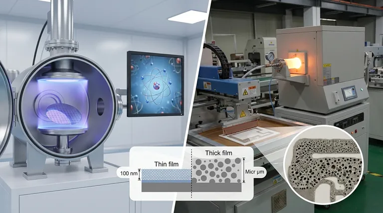
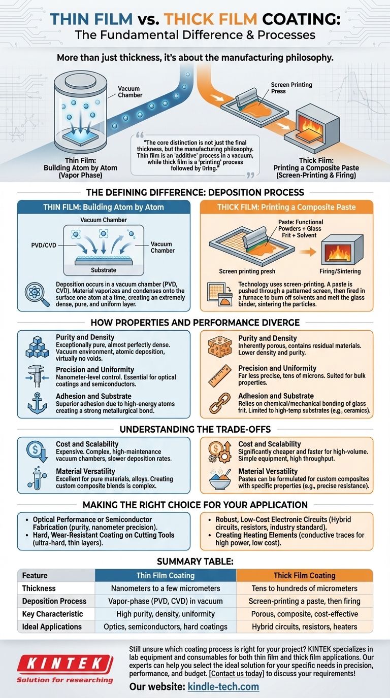
The fundamental difference between thin film and thick film coating lies in their thickness and, more importantly, the process used to create them. Thin films are typically nanometers to a few micrometers thick and are deposited atom-by-atom from a vapor phase. In contrast, thick films are tens to hundreds of micrometers thick and are applied as a screen-printable paste.
The core distinction is not just the final thickness, but the manufacturing philosophy. Thin film is an "additive" process building a solid layer from individual atoms in a vacuum, while thick film is a "printing" process applying a liquid-like paste that is then fired to form a solid.
The Defining Difference: Deposition Process
The method of application dictates nearly every characteristic of the final coating, from its purity and density to its cost and potential uses.
Thin Film: Building Atom by Atom
Thin film deposition occurs in a vacuum chamber. Processes like Physical Vapor Deposition (PVD) or Chemical Vapor Deposition (CVD) are used.
In these methods, material is vaporized and then condenses onto the substrate surface one atom or molecule at a time. This atomic-level construction creates an extremely dense, pure, and uniform layer.
Thick Film: Printing a Composite Paste
Thick film technology uses a process similar to screen-printing. A special "ink" or paste, which is a mixture of functional powders, a glass frit binder, and an organic solvent, is pushed through a patterned screen onto a substrate.
After printing, the part is heated in a furnace. This firing process burns off the organic solvent and melts the glass binder, which sinters the functional particles together into a solid, cohesive film.
How Properties and Performance Diverge
The dramatic difference in deposition methods leads to coatings with fundamentally different characteristics.
Purity and Density
Thin films are exceptionally pure and almost perfectly dense. The vacuum environment prevents contamination, and the atomic deposition process leaves virtually no voids in the film structure.
Thick films are inherently porous and contain residual materials from the glass binder. This lower density and purity can impact electrical and mechanical performance compared to a thin film of the same base material.
Precision and Uniformity
Thin film processes offer nanometer-level control over thickness. This precision is essential for applications like optical coatings and semiconductor devices, where even tiny variations can alter performance.
Thick film thickness is far less precise and is typically measured in tens of microns. It is better suited for applications where bulk properties are more important than microscopic precision.
Adhesion and Substrate
Thin films often exhibit superior adhesion because the high-energy atoms embed themselves into the substrate surface, creating a strong metallurgical bond.
Thick film adhesion relies on the chemical and mechanical bonding of the glass frit to the substrate during the firing cycle. While this bond is very robust, it is generally limited to substrates that can withstand high firing temperatures, such as ceramics.
Understanding the Trade-offs
Choosing between these technologies is a classic engineering trade-off between performance, complexity, and cost.
Cost and Scalability
Thick film processing is significantly cheaper and faster for high-volume manufacturing. The screen-printing equipment is relatively simple, operates at atmospheric pressure, and has a very high throughput.
Thin film deposition is expensive. It requires complex, high-maintenance vacuum chambers, and the deposition rates are much slower, making it a more costly and time-consuming process.
Material Versatility
Thick film pastes can be formulated by mixing various powders to create custom composites with specific electrical or mechanical properties, such as a precise resistance value.
Thin film methods are excellent for depositing pure materials, alloys, and certain compounds. However, creating custom composite blends is significantly more complex than simply mixing a paste.
Making the Right Choice for Your Application
Your decision should be driven by the primary performance requirement of your component.
- If your primary focus is optical performance or semiconductor fabrication: Thin film is the only choice due to its required purity, uniformity, and nanometer-scale precision.
- If your primary focus is creating robust, low-cost electronic circuits (like hybrid circuits or resistors): Thick film is the industry standard for its cost-effectiveness and scalability.
- If your primary focus is a hard, wear-resistant coating on cutting tools: Thin film processes like PVD are used to create ultra-hard, thin layers (e.g., Titanium Nitride) that don't alter the tool's dimensions.
- If your primary focus is creating heating elements on a ceramic or glass substrate: Thick film is the ideal choice for printing conductive traces that can handle high power at a low cost.
Ultimately, understanding the core process—building from vapor versus printing a paste—empowers you to select the technology that aligns perfectly with your project's goals.
Summary Table:
| Feature | Thin Film Coating | Thick Film Coating |
|---|---|---|
| Thickness | Nanometers to a few micrometers | Tens to hundreds of micrometers |
| Deposition Process | Vapor-phase (PVD, CVD) in vacuum | Screen-printing a paste, then firing |
| Key Characteristic | High purity, density, uniformity | Porous, composite, cost-effective |
| Ideal Applications | Optics, semiconductors, hard coatings | Hybrid circuits, resistors, heaters |
Still unsure which coating process is right for your project? KINTEK specializes in lab equipment and consumables for both thin film and thick film applications. Our experts can help you select the ideal solution for your specific needs in precision, performance, and budget. Contact us today to discuss your requirements!
Visual Guide
Related Products
- Aluminized Ceramic Evaporation Boat for Thin Film Deposition
- Electron Beam Evaporation Coating Oxygen-Free Copper Crucible and Evaporation Boat
- Tungsten Evaporation Boat for Thin Film Deposition
- Molybdenum Tungsten Tantalum Evaporation Boat for High Temperature Applications
- Aluminum-Plastic Flexible Packaging Film for Lithium Battery Packaging
People Also Ask
- Why is an alumina boat selected for catalyst precursors? Ensure Sample Purity at 1000 °C
- What is thin film deposition? Unlock Advanced Surface Engineering for Your Materials
- Why are high-purity ceramic boats used for lignin activation? Ensure Purity & Thermal Stability
- What are the applications of thin films deposition? Unlock New Possibilities for Your Materials
- What is the chemical method for thin film deposition? Build Films from the Molecular Level Up


