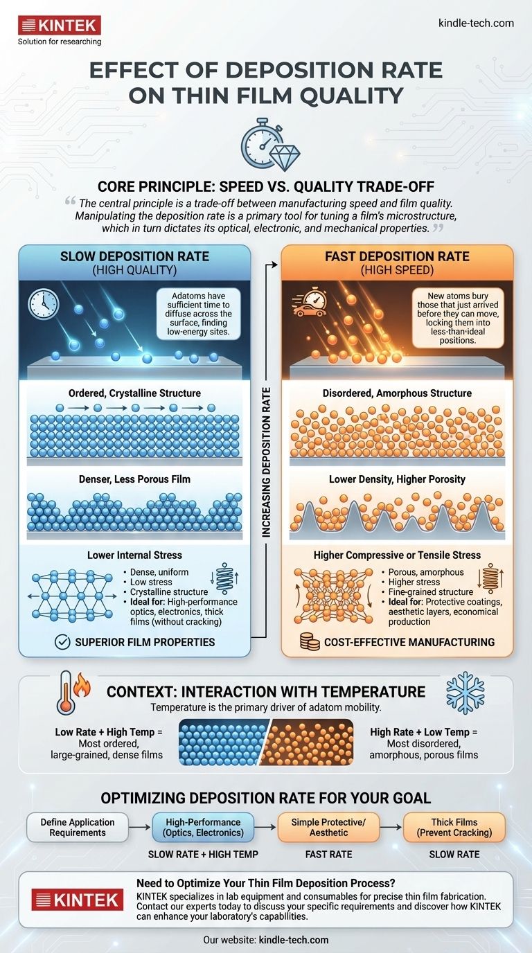
At its core, the deposition rate is a critical control parameter that directly influences a thin film's fundamental physical structure. A higher deposition rate generally results in a more disordered and potentially porous film, while a lower rate allows for the formation of a denser, more uniform, and often more crystalline structure by giving atoms more time to settle into ideal positions.
The central principle is a trade-off between manufacturing speed and film quality. Manipulating the deposition rate is a primary tool for tuning a film's microstructure, which in turn dictates its optical, electronic, and mechanical properties.

The Fundamental Trade-off: Time vs. Energy
The effect of deposition rate is best understood as a competition between the arrival time of new atoms and the time atoms already on the surface have to move around. This mobility is the key to forming a high-quality film.
How Deposition Rate Governs Microstructure
A slow deposition rate provides arriving atoms (adatoms) with sufficient time to diffuse across the substrate surface. This allows them to find low-energy sites, resulting in a more ordered, crystalline, and stable grain structure.
Conversely, a high deposition rate bombards the surface quickly. New atoms bury the ones that have just arrived before they have a chance to move, locking them into less-than-ideal positions. This tends to create a more disordered, amorphous, or fine-grained film structure.
Impact on Film Density and Porosity
Slow deposition allows atoms to fill in microscopic valleys and voids on the surface, leading to a denser, less porous film. This is critical for applications requiring barrier properties or specific optical and electronic performance.
Fast deposition can cause a "shadowing" effect, where peaks on the growing film block incoming atoms from reaching the valleys. This process traps voids within the film, resulting in lower density and higher porosity.
The Role in Internal Film Stress
The way atoms are arranged dictates the film's internal stress. A high deposition rate can trap atoms in energetically unfavorable positions, increasing the compressive or tensile stress within the film.
Slower deposition rates often lead to films with lower internal stress because the atomic structure is closer to its equilibrium state. Managing stress is vital to prevent cracking or delamination of the film from the substrate.
Deposition Rate in Context with Other Variables
The deposition rate does not act in isolation. Its effect is magnified or mitigated by other critical process parameters, as hinted at by the importance of the deposition technique, temperature, and materials.
Interaction with Substrate Temperature
Temperature is the primary driver of adatom mobility. A higher substrate temperature gives atoms more energy to move around, which can compensate for a high deposition rate.
- Low Rate + High Temp: Produces the most ordered, large-grained, and dense films.
- High Rate + Low Temp: Produces the most disordered, amorphous, and potentially porous films.
The Influence of Substrate and Target Material
The properties of the substrate surface and the deposited material itself play a significant role. Some materials naturally form ordered structures more easily than others.
The interaction between the deposited atoms and the substrate influences the initial film growth, and the deposition rate determines how that initial structure propagates through the film's thickness.
Understanding the Practical Trade-offs
Choosing the right deposition rate is a balancing act between the desired film characteristics and manufacturing realities.
Speed vs. Quality
The most obvious trade-off is between throughput and quality. A higher deposition rate means faster production and lower cost per part. However, this may come at the expense of the film's performance and durability.
Risk of Poor Stoichiometry
In reactive deposition processes (e.g., depositing a nitride or oxide), the deposition rate must be balanced with the flow of the reactive gas. If the deposition rate is too high, the material may not fully react, leading to a film with the wrong chemical composition (stoichiometry).
Process Control and Stability
Extremely high deposition rates can sometimes lead to process instability, such as overheating the source material or difficulty in maintaining a uniform deposition cloud. Slower, more controlled rates are often more repeatable for high-precision applications like optics and electronics.
Optimizing Deposition Rate for Your Goal
The ideal deposition rate is defined entirely by the application requirements for the finished film.
- If your primary focus is high-performance optics or electronics: You will likely need a slower deposition rate, possibly combined with elevated substrate temperatures, to achieve a dense, stable, and highly uniform film.
- If your primary focus is a simple protective or aesthetic coating: A higher deposition rate is often acceptable and more economical, as minor variations in density or microstructure may not impact performance.
- If your primary focus is depositing thick films without cracking: A slower rate is generally preferred to minimize the buildup of internal stress that can cause mechanical failure.
Ultimately, controlling the deposition rate is your primary lever for controlling the physical blueprint of the thin film at the atomic level.
Summary Table:
| Deposition Rate | Typical Film Characteristics | Key Applications |
|---|---|---|
| Low Rate | Dense, uniform, low stress, crystalline | High-performance optics, electronics |
| High Rate | Porous, amorphous, higher stress, fine-grained | Protective coatings, aesthetic layers |
Need to Optimize Your Thin Film Deposition Process?
KINTEK specializes in lab equipment and consumables for precise thin film fabrication. Whether you are developing high-performance optical coatings or durable protective layers, our expertise and solutions can help you achieve the ideal microstructure and properties for your application.
Contact our experts today to discuss your specific requirements and discover how KINTEK can enhance your laboratory's capabilities.
Visual Guide
