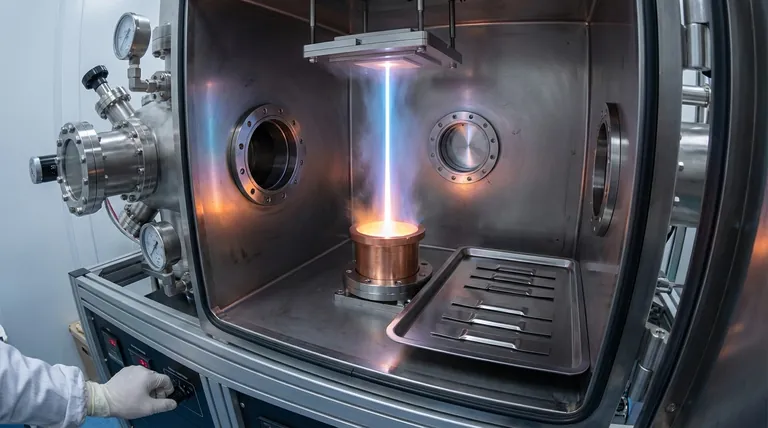
At its core, electron beam (e-beam) evaporation is a physical vapor deposition (PVD) technique that uses a focused beam of high-energy electrons to vaporize a source material inside a high-vacuum chamber. This vaporized material then travels and condenses onto a substrate, forming an exceptionally pure and dense thin film. It is a highly controlled process valued for creating high-performance coatings.
When creating advanced thin films, the central challenge is achieving maximum purity and density. E-beam evaporation solves this by using a precisely controlled electron beam to directly heat only the source material, which minimizes contamination and allows for the deposition of materials with very high melting points.
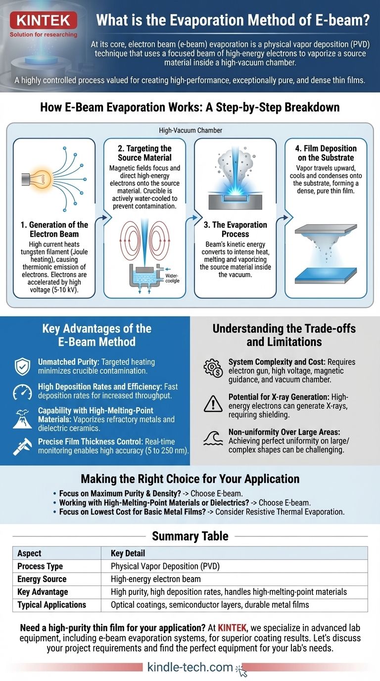
How E-Beam Evaporation Works: A Step-by-Step Breakdown
The e-beam process is a sophisticated method that can be broken down into four distinct stages, from generating electrons to forming the final film.
1. Generation of the Electron Beam
The process begins with a tungsten filament. A high electric current is passed through this filament, causing it to heat up intensely through a process called Joule heating.
This intense heat gives electrons in the tungsten enough energy to escape from its surface, an event known as thermionic emission. These free electrons are then accelerated by a high voltage, typically between 5 and 10 kilovolts (kV).
2. Targeting the Source Material
The high-energy electrons are formed into a focused beam using magnetic fields. This beam is precisely directed at the source material—the substance you wish to deposit—which sits in a crucible.
Critically, this crucible is typically made of copper and is actively water-cooled. This ensures that the intense heat is localized only to the source material, preventing the crucible itself from melting or releasing contaminants.
3. The Evaporation Process
When the high-energy electron beam strikes the source material, its kinetic energy is instantly converted into thermal energy. This creates an incredibly localized and intense hot spot.
This heat first melts the source material and then causes it to evaporate, turning it into a vapor. This entire process must occur within a high-vacuum chamber to prevent the vapor from reacting with air and to allow the vaporized atoms to travel freely.
4. Film Deposition on the Substrate
The vaporized material travels in a straight line upward from the source. It eventually reaches the substrate, which is a cooler surface positioned above the crucible.
Upon hitting the substrate, the vapor rapidly cools and condenses, forming a solid, thin film. The resulting film is dense, strongly adhered, and possesses the high purity of the original source material.
Key Advantages of the E-Beam Method
E-beam evaporation is chosen over other deposition methods for several distinct technical advantages.
Unmatched Purity
Because the electron beam heats only the source material, contamination from the crucible is virtually eliminated. This is a significant advantage over simpler thermal evaporation methods where the entire crucible is heated, often becoming a source of impurities.
High Deposition Rates and Efficiency
The direct transfer of energy from the electron beam to the material is highly efficient. This allows for much faster deposition rates compared to other PVD techniques, improving throughput in manufacturing environments.
Capability with High-Melting-Point Materials
The immense energy concentration of the electron beam makes it one of the few methods capable of vaporizing materials with very high melting points, such as refractory metals (e.g., tungsten, tantalum) and dielectric ceramics.
Precise Film Thickness Control
The rate of evaporation can be precisely monitored and controlled in real-time by adjusting the beam current. This allows for the creation of films with highly accurate and repeatable thickness, often in the range of 5 to 250 nanometers.
Understanding the Trade-offs and Limitations
While powerful, the e-beam method is not without its complexities and is not the right choice for every application.
System Complexity and Cost
An e-beam system requires an electron gun, high-voltage power supplies, magnetic guidance systems, and a high-vacuum chamber. This makes it significantly more complex and expensive to purchase and maintain than simpler methods like resistive thermal evaporation.
Potential for X-ray Generation
The impact of high-energy electrons on a target can generate X-rays. This radiation can sometimes damage sensitive electronic substrates or alter the properties of the film itself, and may require additional shielding for operators.
Non-uniformity Over Large Areas
Achieving a perfectly uniform coating thickness across a large or complexly shaped substrate can be challenging. It often requires sophisticated planetary rotation systems to ensure all surfaces of the substrate are evenly exposed to the vapor stream.
Making the Right Choice for Your Application
The decision to use e-beam evaporation hinges on your specific technical requirements for film quality and material type.
- If your primary focus is maximum film purity and density: E-beam is the superior choice due to its targeted heating that minimizes crucible contamination.
- If you are working with high-melting-point materials or dielectrics: E-beam provides the necessary energy concentration that simpler thermal methods cannot achieve.
- If your primary concern is lowest cost and system simplicity for basic metal films: You might consider standard resistive thermal evaporation as a more economical alternative.
Ultimately, understanding these principles empowers you to select the deposition method that aligns perfectly with your engineering goals.
Summary Table:
| Aspect | Key Detail |
|---|---|
| Process Type | Physical Vapor Deposition (PVD) |
| Energy Source | High-energy electron beam |
| Key Advantage | High purity, high deposition rates, handles high-melting-point materials |
| Typical Applications | Optical coatings, semiconductor layers, durable metal films |
Need a high-purity thin film for your application?
At KINTEK, we specialize in providing advanced lab equipment, including e-beam evaporation systems, to help you achieve superior coating results. Our solutions are designed for precision, reliability, and handling high-performance materials.
Let's discuss your project requirements and find the perfect equipment for your lab's needs.
Contact our experts today for a personalized consultation!
Visual Guide
Related Products
- Electron Beam Evaporation Coating Oxygen-Free Copper Crucible and Evaporation Boat
- Electron Beam Evaporation Coating Tungsten Crucible and Molybdenum Crucible for High Temperature Applications
- Electron Beam Evaporation Coating Gold Plating Tungsten Molybdenum Crucible for Evaporation
- E Beam Crucibles Electron Gun Beam Crucible for Evaporation
- Electron Beam Evaporation Coating Conductive Boron Nitride Crucible BN Crucible
People Also Ask
- How is an electron beam evaporator cooled during deposition? Essential Thermal Management for Stable Processes
- What is the voltage of e-beam evaporation? Achieve Precise Thin-Film Deposition
- What is e-beam evaporation used for? Precision Coating for Optics, Aerospace & Electronics
- What is the deposition rate of e-beam evaporation? Control Thin Film Quality and Speed
- What is the temperature of e-beam evaporation? Mastering the Two-Zone Thermal Process for Precision Films


