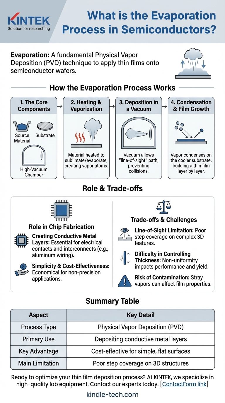
In semiconductor manufacturing, evaporation is a fundamental deposition technique used to apply a thin film of material onto a semiconductor wafer. The process involves heating a source material inside a high-vacuum chamber until it vaporizes. These vaporized atoms or molecules then travel and condense onto the cooler wafer surface, building a new layer. This method is a form of Physical Vapor Deposition (PVD).
Evaporation is essentially a process of "boiling" a material in a vacuum and letting it condense onto a target substrate. While it is a direct and often cost-effective way to create thin films, its primary trade-off is a lack of precise control over film thickness and uniformity compared to more advanced techniques.
How the Evaporation Process Works
To understand its role, it's helpful to break down the process into its core mechanical steps. The entire operation takes place within a specialized, highly controlled environment.
The Core Components
The system consists of three main parts: the source material (e.g., a metal like aluminum), the substrate (the semiconductor wafer to be coated), and a high-vacuum chamber that encloses them.
The Heating and Vaporization Phase
The source material is heated to a high temperature, causing it to sublimate or evaporate, transitioning directly into a gaseous phase. This creates a cloud of vaporized atoms.
Deposition in a Vacuum
The vacuum is critical. By removing most air molecules, it ensures the vaporized source atoms can travel in a straight, uninterrupted path—a "line-of-sight"—from the source to the substrate. This prevents them from colliding with air particles, which would cause them to scatter or react.
Condensation and Film Growth
When the hot vapor atoms strike the much cooler surface of the semiconductor wafer, they rapidly lose energy and condense back into a solid state. This process gradually builds up a thin, solid film on the substrate, layer by layer.
The Role of Evaporation in Chip Fabrication
Evaporation is not used for every layer on a modern chip, but it remains a valuable tool for specific applications where its characteristics are a good fit.
Creating Conductive Metal Layers
A primary use for evaporation is depositing metal films, particularly for creating electrical contacts and interconnects. For example, it's a common method for laying down the aluminum "wiring" that connects various transistors and components across a chip.
Simplicity and Cost-Effectiveness
Compared to more complex deposition methods, the equipment and process for thermal evaporation can be relatively simple and less expensive. This makes it an economical choice for applications that do not require atomic-level precision.
Understanding the Trade-offs and Challenges
While effective, evaporation has clear limitations that have led to the development of other deposition techniques for more demanding process steps.
The "Line-of-Sight" Limitation
Because the material vapor travels in a straight line, it struggles to evenly coat complex, three-dimensional surface features. This results in poor "step coverage," where the film is much thinner on the sidewalls of a trench than on its top surface.
Difficulty in Controlling Thickness
The rate of evaporation can be challenging to control with high precision. This can lead to non-uniform film thickness across the wafer and from one wafer to the next, impacting device performance and yield.
The Risk of Contamination
Any component inside the vacuum chamber that gets hot can release unwanted vapors. These stray molecules can co-deposit with the source material, contaminating the film and altering its electrical or physical properties, ultimately reducing its quality.
Making the Right Choice for Your Goal
Selecting a deposition method depends entirely on the technical requirements of the film you are creating.
- If your primary focus is cost-effective metal coatings on flat surfaces: Evaporation is a highly suitable and economical choice for creating simple contacts or bonding pads.
- If your primary focus is coating complex 3D structures with high uniformity: You should explore alternative PVD methods like sputtering, which does not have the same line-of-sight limitation and offers superior step coverage.
- If your primary focus is depositing films with precise composition or low contamination: More advanced techniques like sputtering or Chemical Vapor Deposition (CVD) offer much tighter control over these critical parameters.
Understanding the fundamental trade-offs of evaporation is key to selecting the right fabrication process for your specific semiconductor device.
Summary Table:
| Aspect | Key Detail |
|---|---|
| Process Type | Physical Vapor Deposition (PVD) |
| Primary Use | Depositing conductive metal layers (e.g., aluminum contacts) |
| Key Advantage | Cost-effective for simple, flat surface coatings |
| Main Limitation | Poor step coverage on 3D structures due to line-of-sight deposition |
Ready to optimize your thin film deposition process?
The evaporation process is just one tool for semiconductor fabrication. Choosing the right equipment is critical for yield and performance.
At KINTEK, we specialize in high-quality lab equipment, including deposition systems, to meet the precise needs of semiconductor R&D and production. Our expertise helps you select the right technology for your specific application, whether it's cost-effective evaporation or advanced solutions for complex structures.
Let's discuss your project requirements and find the perfect solution for your lab. Contact our experts today to enhance your fabrication capabilities.
Visual Guide
Related Products
- Molybdenum Tungsten Tantalum Evaporation Boat for High Temperature Applications
- Aluminized Ceramic Evaporation Boat for Thin Film Deposition
- Evaporation Boat for Organic Matter
- Multi Heating Zones CVD Tube Furnace Machine Chemical Vapor Deposition Chamber System Equipment
- Chemical Vapor Deposition CVD Equipment System Chamber Slide PECVD Tube Furnace with Liquid Gasifier PECVD Machine
People Also Ask
- How source material is evaporated during deposition? A Guide to Resistive vs. E-Beam Methods
- What is the source of evaporation for thin film? Choosing Between Thermal and E-Beam Methods
- What is the difference between thermal evaporation and e beam evaporation? Choose the Right Method for Your Thin Film
- What are thermal evaporation sources? Key Types and How to Choose the Right One
- Is thermal evaporation used to deposit a thin metal film? A Guide to This Foundational PVD Technique