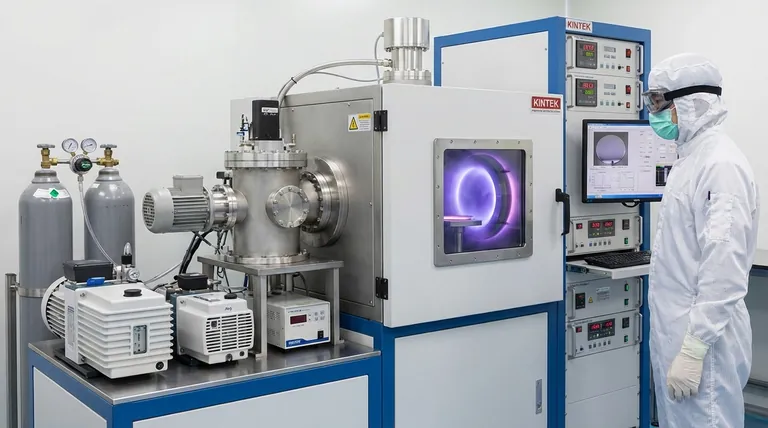
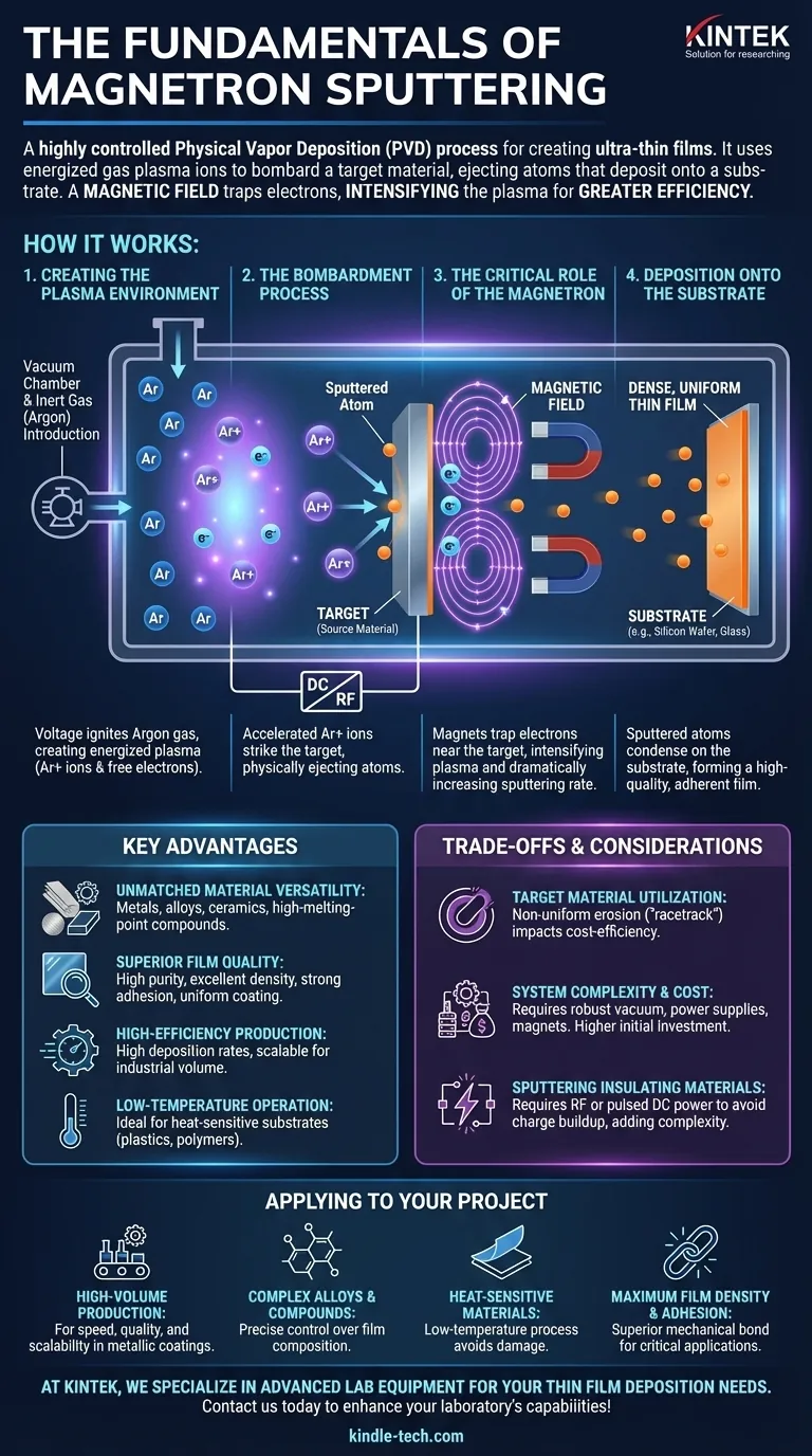
At its core, magnetron sputtering is a highly controlled physical vapor deposition (PVD) process used to create ultra-thin films. The technique involves bombarding a source material, known as the "target," with energized ions from a gas plasma. This bombardment physically knocks atoms off the target, which then travel and deposit onto a substrate, forming a dense and uniform coating. The "magnetron" aspect is the key innovation: a magnetic field is used to trap electrons near the target, dramatically intensifying the plasma and making the entire process vastly more efficient.
The fundamental advantage of magnetron sputtering is its ability to create high-quality, dense, and uniform thin films from nearly any material at high speeds and low temperatures. It achieves this by using magnetic fields to intensify a plasma, creating a highly efficient and controllable deposition process that is ideal for industrial-scale applications.
How Magnetron Sputtering Works: From Plasma to Film
To understand why this technique is so powerful, we must first break down the process step-by-step. It is a precise sequence of events occurring within a vacuum chamber.
Creating the Plasma Environment
First, a vacuum chamber is pumped down to a very low pressure. A small amount of an inert gas, typically Argon (Ar), is then introduced. A high voltage is applied between the target material (which acts as the cathode) and the chamber/anode.
This voltage ignites the gas, stripping electrons from the Argon atoms and creating a plasma—a glowing, energized soup of positive Argon ions (Ar+) and free electrons.
The Bombardment Process
The positively charged Argon ions are accelerated by the electric field and slam into the negatively charged target surface with significant kinetic energy.
Each collision is energetic enough to physically eject, or "sputter," atoms from the target material. These ejected atoms travel in a straight line away from the target.
The Critical Role of the Magnetron
This is where the technique gains its efficiency. Magnets are placed behind the target. This magnetic field traps the much lighter electrons, forcing them into a spiral path directly in front of the target's surface.
Without the magnetic field, electrons would be quickly lost. By trapping them, the probability of them colliding with and ionizing more Argon atoms increases exponentially. This creates a much denser, more intense plasma right where it's needed, which dramatically increases the sputtering rate.
Deposition onto the Substrate
The sputtered atoms from the target travel through the vacuum chamber and condense on the surface of a substrate (such as a silicon wafer, glass, or plastic part) placed in their path.
Because these atoms arrive with significant kinetic energy, they can embed slightly into the surface and arrange themselves into a very dense, pure, and highly adherent film.
Why This Process is So Effective: Key Advantages
The physics of the magnetron sputtering process directly leads to a set of advantages that make it a go-to choice for advanced manufacturing.
Unmatched Material Versatility
The process is purely physical, not thermal. It does not require melting or evaporating the source material.
This allows for the deposition of virtually any material, including metals, alloys, ceramics, and compounds with extremely high melting points that are impossible to deposit using other methods.
Superior Film Quality
The high energy of the sputtered atoms results in films with exceptional properties. They are known for their high purity, excellent density, and extremely strong adhesion to the substrate.
Furthermore, the process allows for highly uniform coating over large areas, which is critical for applications like semiconductors and architectural glass.
High-Efficiency Production
The magnetic confinement of the plasma leads to very high deposition rates, especially for metals.
This speed, combined with excellent uniformity and the potential for full automation, makes magnetron sputtering highly scalable and ideal for high-volume industrial production.
Low-Temperature Operation
Because the substrate is not intentionally heated, sputtering is a low-temperature process. This is a crucial advantage for coating heat-sensitive substrates like plastics, polymers, and fabrics without causing damage.
Understanding the Trade-offs and Considerations
No technique is perfect. To use magnetron sputtering effectively, you must be aware of its inherent limitations.
Target Material Utilization
The magnetic field that enhances the plasma also confines it to a specific region on the target. This leads to non-uniform erosion of the target material in a pattern often called a "racetrack."
This means that a significant portion of the expensive target material may not be consumed, impacting cost-efficiency over time.
System Complexity and Cost
A magnetron sputtering system is more complex than a simple thermal evaporator. It requires a robust vacuum system, high-voltage DC or RF power supplies, and precisely engineered magnet assemblies. This translates to higher initial capital investment.
Sputtering Insulating Materials
While sputtering can deposit dielectrics (insulators), it requires a specific approach. Using a standard DC power supply causes a positive charge buildup on the insulating target, which repels the Argon ions and quickly stops the process.
This is overcome by using Radio Frequency (RF) or pulsed DC power supplies, which rapidly alternate the voltage to neutralize the charge buildup. However, this adds complexity and cost, and deposition rates for dielectrics are typically lower than for metals.
How to Apply This to Your Project
Your choice of deposition technology should always align with your end goal. Magnetron sputtering excels in several key areas.
- If your primary focus is high-volume production of metallic coatings: Magnetron sputtering offers an unmatched combination of deposition speed, film quality, and industrial scalability.
- If your primary focus is depositing complex alloys or novel compounds: Co-sputtering from multiple targets or reactive sputtering in a gas mixture (e.g., nitrogen or oxygen) provides precise control over film composition.
- If your primary focus is coating heat-sensitive materials: The low-temperature nature of the process makes it an ideal choice over thermal methods that would damage plastics or polymers.
- If your primary focus is achieving maximum film density and adhesion: The high kinetic energy of sputtered atoms ensures a superior mechanical bond and film integrity compared to most other PVD techniques.
By mastering a controlled plasma with magnetic fields, magnetron sputtering provides an unparalleled and versatile tool for engineering surfaces at the atomic level.
Summary Table:
| Key Aspect | Benefit |
|---|---|
| Process Type | Physical Vapor Deposition (PVD) |
| Core Mechanism | Magnetic field traps electrons to intensify plasma |
| Primary Use | Creating ultra-thin, dense, and uniform coatings |
| Material Versatility | Works with metals, alloys, ceramics, and high-melting-point compounds |
| Key Advantage | High deposition rates, excellent adhesion, and low-temperature operation |
| Ideal For | Semiconductors, architectural glass, and heat-sensitive substrates like plastics |
Ready to engineer superior surfaces with precision?
At KINTEK, we specialize in providing advanced lab equipment and consumables tailored to your thin film deposition needs. Whether you're working on semiconductors, coating heat-sensitive materials, or developing novel compounds, our magnetron sputtering solutions deliver the high-quality, dense, and uniform films your research or production requires.
Contact us today to discuss how our expertise can enhance your laboratory's capabilities and drive your projects forward!
Visual Guide
Related Products
- Spark Plasma Sintering Furnace SPS Furnace
- RF PECVD System Radio Frequency Plasma-Enhanced Chemical Vapor Deposition RF PECVD
People Also Ask
- What is the pressure for spark plasma sintering? A Guide to Optimizing SPS Parameters
- What are the advantages of CAMI/SPS for W-Cu composite preparation? Reduce cycles from hours to seconds.
- What technical advantages does a Spark Plasma Sintering (SPS) furnace offer for LZP ceramics? Enhance Ionic Conductivity
- What is the process fundamentals of spark plasma sintering? Achieve Rapid, High-Density Material Consolidation
- What is the theory of spark plasma sintering? A Guide to Rapid, Low-Temperature Densification

