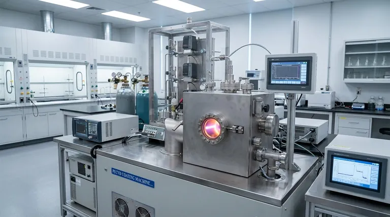
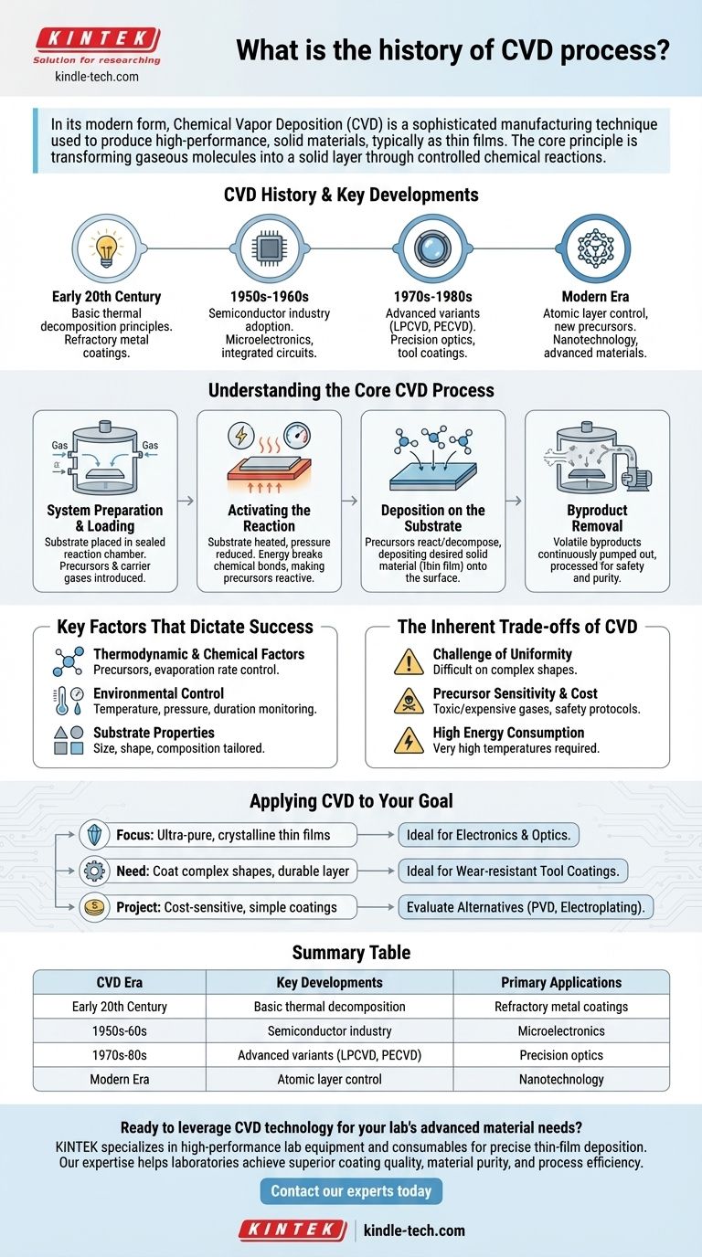
In its modern form, Chemical Vapor Deposition (CVD) is a sophisticated manufacturing technique used to produce high-performance, solid materials, typically as thin films. The process involves placing a substrate within a reaction chamber and introducing specific precursor gases, which then decompose or react on the heated substrate surface to create the desired coating. This method is fundamental to industries like semiconductor manufacturing and material science.
The core principle of CVD is transforming gaseous molecules into a solid layer on a surface through controlled chemical reactions. Successfully mastering this process depends entirely on precise control over variables like temperature, pressure, and gas composition.
Understanding the Core CVD Process
Chemical Vapor Deposition is not a single action but a sequence of carefully managed steps. The goal is to build a new material layer atom-by-atom or molecule-by-molecule, resulting in a highly pure and structured film.
Step 1: System Preparation and Loading
The foundation of any successful CVD run is preparing the reaction environment. A substrate, which is the material to be coated, is placed inside a sealed reaction chamber. A mixture of volatile precursors (the gases containing the atoms you want to deposit) and inert carrier gases is then introduced.
Step 2: Activating the Reaction
To initiate the chemical process, energy is introduced into the system. The substrate is heated to a specific temperature, and the chamber pressure is reduced. This combination provides the necessary energy to break the chemical bonds in the precursor gases, making them reactive.
Step 3: Deposition on the Substrate
Once activated, the precursor gases decompose or react near the hot substrate. This chemical reaction results in the desired solid material being deposited onto the substrate's surface, forming a thin-film coating. The structure and properties of this film are determined by the reaction conditions.
Step 4: Byproduct Removal
The chemical reactions also create volatile byproducts that are no longer needed. These gaseous waste products are continuously pumped out of the chamber. They are then processed to prevent environmental pollution and ensure the purity of the deposition process.
Key Factors That Dictate Success
The final quality of a CVD film is not accidental; it is the direct result of managing several critical process parameters. A small deviation in any single factor can dramatically alter the outcome.
Thermodynamic and Chemical Factors
The specific precursors used and the thermodynamics of the desired material are fundamental. The evaporation rate of the precursors must be tightly controlled to achieve a specific film thickness or composition.
Environmental Control
Variables like temperature, pressure, and the duration of the deposition must be carefully monitored and maintained. These factors directly influence the reaction rates and the final structure of the deposited film.
Substrate Properties
The size, shape, and composition of the substrate itself also play a crucial role. The process must be tailored to the specific object being coated to ensure uniform and adhesive deposition.
The Inherent Trade-offs of CVD
While powerful, the CVD process presents significant challenges that require careful management. Understanding these complexities is key to its successful application.
The Challenge of Uniformity
Achieving a perfectly uniform coating, especially on complex, three-dimensional shapes, is a primary difficulty. Variations in temperature or gas flow across the substrate can lead to inconsistencies in film thickness and quality.
Precursor Sensitivity and Cost
The precursor gases used in CVD can be highly toxic, flammable, or expensive. Handling and sourcing these materials adds complexity and cost to the process, requiring specialized equipment and safety protocols.
High Energy Consumption
Most CVD processes require very high temperatures to activate the necessary chemical reactions. This results in significant energy consumption, which can be a major economic consideration, particularly for large-scale production.
Applying CVD to Your Goal
The decision to use CVD should be based on a clear understanding of what it excels at providing. It is a precision tool for specific material engineering challenges.
- If your primary focus is creating ultra-pure, crystalline thin films: CVD is an industry standard, particularly in electronics and optics where material purity is non-negotiable.
- If you need to coat complex shapes with a durable, high-performance layer: The gaseous nature of the process allows it to deposit conformal coatings, making it ideal for applications like wear-resistant tool coatings.
- If your project is highly cost-sensitive and requires simple coatings: You may need to evaluate alternative, lower-temperature, and less complex methods like Physical Vapor Deposition (PVD) or electroplating.
Ultimately, CVD is a foundational technology for building the high-performance materials that drive modern innovation.
Summary Table:
| CVD Era | Key Developments | Primary Applications |
|---|---|---|
| Early 20th Century | Basic thermal decomposition principles | Refractory metal coatings |
| 1950s-1960s | Semiconductor industry adoption | Microelectronics, integrated circuits |
| 1970s-1980s | Advanced variants (LPCVD, PECVD) | Precision optics, tool coatings |
| Modern Era | Atomic layer control, new precursors | Nanotechnology, advanced materials |
Ready to leverage CVD technology for your lab's advanced material needs? KINTEK specializes in high-performance lab equipment and consumables for precise thin-film deposition. Our expertise in CVD systems helps laboratories achieve superior coating quality, material purity, and process efficiency. Contact our experts today to discuss how our CVD solutions can accelerate your research and manufacturing outcomes!
Visual Guide
Related Products
- CVD Diamond Dressing Tools for Precision Applications
- Multi Heating Zones CVD Tube Furnace Machine Chemical Vapor Deposition Chamber System Equipment
- CVD Diamond Domes for Industrial and Scientific Applications
- CVD Diamond for Thermal Management Applications
- Chemical Vapor Deposition CVD Equipment System Chamber Slide PECVD Tube Furnace with Liquid Gasifier PECVD Machine
People Also Ask
- What are the raw materials for CVD diamonds? A seed, a gas, and the science of crystal growth.
- What color diamonds are CVD? Understanding the Process from Brown Tint to Colorless Beauty
- How do you identify a CVD diamond? The Definitive Guide to Lab-Grown Diamond Verification
- How do CVD diamonds grow? A Step-by-Step Guide to Lab-Grown Diamond Creation
- How long does it take to make synthetic diamonds? Discover the 6-8 Week Science Behind Lab-Grown Gems


