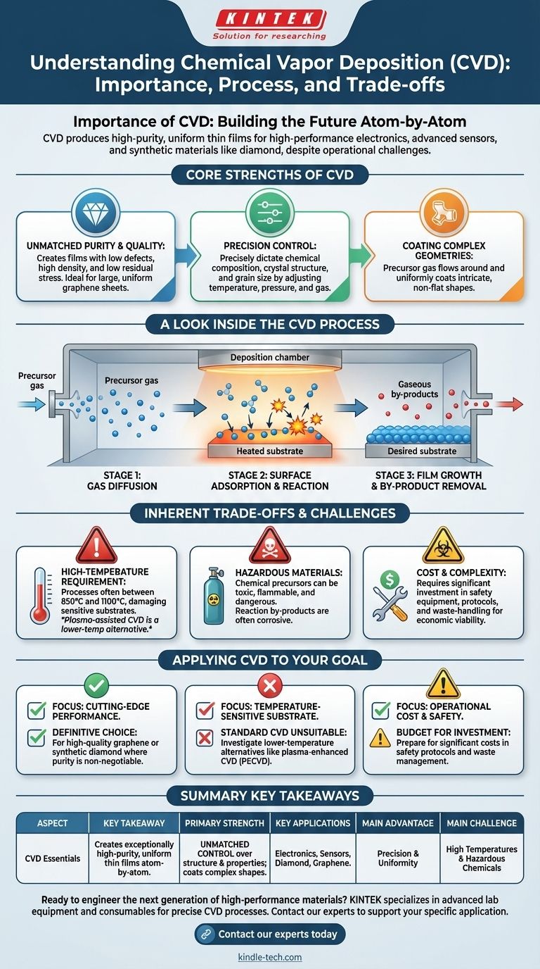
At its core, Chemical Vapor Deposition (CVD) is one of the most important modern techniques for building materials atom-by-atom. Its significance comes from its ability to produce exceptionally high-purity, uniform thin films and coatings, which are foundational to high-performance electronics, advanced sensors, and synthetic materials like diamond.
CVD offers unparalleled control over the structure and purity of a material at the microscopic level. This precision makes it a leading manufacturing approach for next-generation technologies, but it comes with significant operational challenges, primarily high temperatures and hazardous chemicals.
The Core Strengths of CVD
The importance of CVD stems from a unique combination of capabilities that are difficult to achieve with other methods. These strengths make it the preferred choice for applications demanding the highest material quality.
Unmatched Purity and Quality
CVD can produce films with extremely high purity and a low count of structural defects. This results in dense, well-crystallized layers with low residual stress.
This level of quality is why CVD is the leading approach for manufacturing large, uniform sheets of graphene for advanced electronics.
Precision Control Over Material Properties
By carefully adjusting deposition parameters like temperature, pressure, and gas composition, operators can precisely control the final material.
This includes dictating the chemical composition, crystal structure, and grain size of the deposited film, tailoring it for specific performance requirements.
Coating Complex Geometries
The process relies on a precursor gas that can flow around and coat intricate shapes uniformly.
This "wrap-around" capability is a significant advantage for depositing protective or functional layers on complex, non-flat components.
A Look Inside the CVD Process
Understanding the process reveals why CVD can achieve such high-quality results. The deposition occurs in three distinct stages on the surface of a substrate.
Stage 1: Gas Diffusion
A precursor gas, which contains the atoms needed for the final film, is introduced into a reaction chamber. This gas diffuses through the chamber and moves toward the substrate's surface.
Stage 2: Surface Adsorption and Reaction
The gas molecules are adsorbed onto the hot surface of the substrate. The thermal energy at the surface then triggers a chemical reaction.
Stage 3: Film Growth and By-product Removal
This chemical reaction forms the desired solid material, which grows as a thin film on the substrate. Gaseous by-products from the reaction are then released and swept away.
Understanding the Inherent Trade-offs
While powerful, CVD is not a universal solution. Its precision comes with significant operational and safety challenges that must be carefully managed.
The High-Temperature Requirement
Traditional CVD processes operate at very high temperatures, often between 850°C and 1100°C.
This heat can damage or destroy many substrate materials, limiting its application. However, newer techniques like plasma-assisted CVD can lower this temperature requirement.
The Challenge of Hazardous Materials
The chemical precursors required for CVD often have high vapor pressure and can be highly toxic, flammable, or dangerous to handle.
Furthermore, the gaseous by-products of the reaction are frequently toxic and corrosive, posing a significant safety and environmental risk.
Cost and Complexity of Mitigation
The need to handle hazardous materials safely and neutralize toxic by-products adds significant cost and complexity to the CVD process. This is a critical factor in determining its economic viability for a given application.
Applying CVD to Your Goal
Your decision to use or specify CVD depends entirely on whether its benefits outweigh its considerable demands.
- If your primary focus is cutting-edge material performance: CVD is the definitive choice for applications like high-quality graphene or synthetic diamond where purity and structural perfection are non-negotiable.
- If your primary focus is coating a temperature-sensitive substrate: Standard CVD is likely unsuitable, and you must investigate lower-temperature alternatives like plasma-enhanced CVD (PECVD).
- If your primary focus is operational cost and safety: You must budget for significant investment in equipment, safety protocols, and waste-handling to manage the hazardous chemicals and high temperatures involved.
Ultimately, Chemical Vapor Deposition is a demanding but uniquely capable tool for engineering the high-performance materials that drive technological progress.
Summary Table:
| Aspect | Key Takeaway |
|---|---|
| Primary Strength | Creates exceptionally high-purity, uniform thin films atom-by-atom. |
| Key Applications | High-performance electronics, advanced sensors, synthetic diamond, graphene. |
| Main Advantage | Unmatched control over material structure and properties; coats complex 3D shapes. |
| Main Challenge | High operating temperatures and the use of hazardous chemical precursors. |
Ready to engineer the next generation of high-performance materials?
KINTEK specializes in providing the advanced lab equipment and consumables needed for precise Chemical Vapor Deposition processes. Whether you are developing cutting-edge electronics or require coatings for complex components, our expertise can help you achieve the material purity and performance your research demands.
Contact our experts today to discuss how we can support your specific CVD application and laboratory needs.
Visual Guide
Related Products
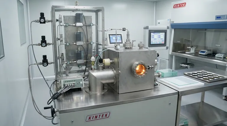
- Chemical Vapor Deposition CVD Equipment System Chamber Slide PECVD Tube Furnace with Liquid Gasifier PECVD Machine
- RF PECVD System Radio Frequency Plasma-Enhanced Chemical Vapor Deposition RF PECVD
- Microwave Plasma Chemical Vapor Deposition MPCVD Machine System Reactor for Lab and Diamond Growth
- Customer Made Versatile CVD Tube Furnace Chemical Vapor Deposition Chamber System Equipment
- 915MHz MPCVD Diamond Machine Microwave Plasma Chemical Vapor Deposition System Reactor
People Also Ask
- What happens during deposition chemistry? Building Thin Films from Gaseous Precursors
- What are the processes of vapor phase deposition? Understand CVD vs. PVD for Superior Thin Films
- Why is Chemical Vapor Deposition (CVD) equipment uniquely suited for constructing hierarchical superhydrophobic structures?
- What is the chemical vapor deposition growth process? Build Superior Thin Films from the Atom Up
- What are the advantages of chemical vapor deposition? Achieve Superior Thin Films for Your Lab


