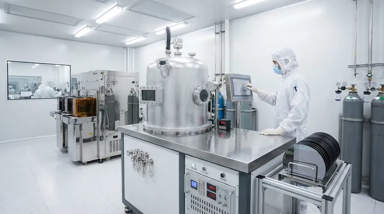
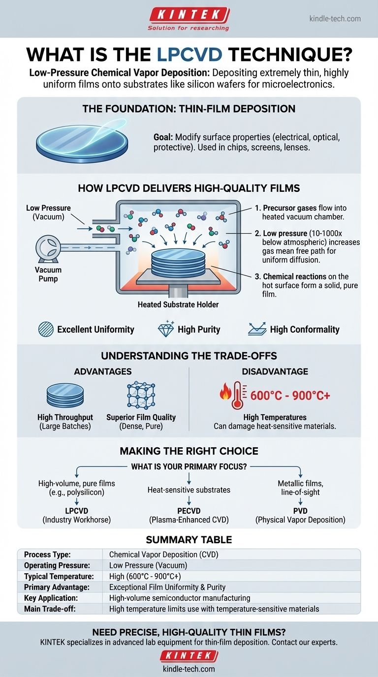
In short, Low-Pressure Chemical Vapor Deposition (LPCVD) is a specific process used to deposit extremely thin, highly uniform layers of material onto a substrate, such as a silicon wafer. It operates under a vacuum and uses heat to trigger chemical reactions from precursor gases, resulting in a solid film that coats the substrate. LPCVD is a cornerstone of modern manufacturing, especially for semiconductors and microelectronics.
While many techniques exist for applying thin films, LPCVD is the go-to method for achieving exceptional film purity and uniformity over large batches of substrates. Its primary trade-off is the high temperature required, which dictates when and where it can be used in a manufacturing sequence.
The Foundation: Understanding Thin-Film Deposition
Before diving deeper into LPCVD, it's essential to understand the broader field it belongs to: thin-film deposition.
The Goal: Modifying Surface Properties
Thin-film deposition is a foundational industrial process for applying a thin coating—from a few nanometers to several micrometers thick—onto a target material, known as a substrate.
The purpose is to fundamentally change the surface properties of that substrate. These coatings can alter electrical conductivity, provide corrosion resistance, increase hardness, or change optical characteristics.
A Critical Process in Modern Technology
This technique is not niche; it's a critical step in manufacturing countless items. You can find its results in semiconductor chips, smartphone screens, specialized optical lenses, and protective coatings on automotive parts.
The deposited films can be made of various materials, including metals, oxides, nitrides, and other compounds, each chosen to impart a specific desired quality to the final product.
How LPCVD Delivers High-Quality Films
LPCVD is a specific and highly refined method of chemical vapor deposition (CVD). Its name reveals its core operating principles.
The Core Principle: Chemical Vapor Deposition
At its heart, Chemical Vapor Deposition (CVD) involves introducing one or more volatile precursor gases into a reaction chamber. When these gases come into contact with a heated substrate, they react or decompose, leaving a solid material behind as a thin film on the substrate's surface.
The "Low Pressure" Advantage
The "Low Pressure" in LPCVD is the key differentiator. The process takes place in a chamber under a vacuum (low pressure), typically 10 to 1,000 times lower than atmospheric pressure.
Reducing the pressure significantly increases the mean free path of the gas molecules. This allows them to travel farther and more freely before colliding, ensuring they can diffuse evenly across all substrate surfaces, even in densely packed batches.
The Result: Uniformity and Purity
This low-pressure environment leads to two critical benefits. First, it results in films with excellent uniformity across the entire substrate. Second, it reduces the chance of gas-phase reactions that create unwanted particles, leading to films of very high purity.
The process is surface-reaction limited, meaning the deposition rate is controlled by the chemical reaction on the hot substrate, not by how fast gas can get there. This ensures that even complex, three-dimensional structures are coated evenly—a property known as high conformality.
Understanding the Trade-offs
No technique is perfect for every application. The strengths and weaknesses of LPCVD define its role in manufacturing.
Key Advantage: High Throughput and Conformality
Because of the excellent gas diffusion at low pressure, LPCVD systems can process large batches of wafers—often 100 to 200 at a time—stacked vertically in a furnace. This high throughput makes it exceptionally cost-effective for high-volume production. Its conformality is essential for creating complex microelectronic devices.
Key Advantage: Superior Film Quality
LPCVD produces films that are dense, pure, and have excellent electrical properties. For materials like polysilicon, silicon nitride, and silicon dioxide, it is the industry standard for achieving the required quality in semiconductor manufacturing.
Primary Disadvantage: High Temperatures
The main limitation of LPCVD is its reliance on high temperatures, typically ranging from 600°C to over 900°C. This heat can damage or alter other materials or devices already present on the substrate, such as aluminum interconnects. This means it must be used strategically, often early in the fabrication process before temperature-sensitive components are added.
Making the Right Choice for Your Goal
Selecting a deposition technique requires matching the process capabilities to your specific material and device requirements.
- If your primary focus is high-volume production of extremely pure and uniform films like polysilicon or silicon nitride: LPCVD is the undisputed industry workhorse for this task.
- If your primary focus is depositing films onto substrates that cannot withstand high heat: A lower-temperature method like Plasma-Enhanced CVD (PECVD) is the more appropriate choice.
- If your primary focus is depositing pure metallic films where line-of-sight deposition is acceptable: A Physical Vapor Deposition (PVD) technique like sputtering might be more suitable.
Ultimately, choosing the right method is about understanding the critical trade-off between film quality, process temperature, and throughput for your specific application.
Summary Table:
| Key Aspect | LPCVD Characteristic |
|---|---|
| Process Type | Chemical Vapor Deposition (CVD) |
| Operating Pressure | Low Pressure (Vacuum) |
| Typical Temperature | High (600°C - 900°C+) |
| Primary Advantage | Exceptional Film Uniformity & Purity |
| Key Application | High-volume semiconductor manufacturing (e.g., polysilicon, silicon nitride) |
| Main Trade-off | High temperature limits use with temperature-sensitive materials |
Need precise, high-quality thin films for your laboratory or production line? KINTEK specializes in providing advanced lab equipment and consumables for thin-film deposition and other critical processes. Our expertise can help you select the right technology to achieve superior film uniformity and purity for your specific application. Contact our experts today to discuss how we can support your laboratory's success!
Visual Guide
Related Products
- Chemical Vapor Deposition CVD Equipment System Chamber Slide PECVD Tube Furnace with Liquid Gasifier PECVD Machine
- Inclined Rotary Plasma Enhanced Chemical Vapor Deposition PECVD Equipment Tube Furnace Machine
- RF PECVD System Radio Frequency Plasma-Enhanced Chemical Vapor Deposition RF PECVD
- Microwave Plasma Chemical Vapor Deposition MPCVD Machine System Reactor for Lab and Diamond Growth
- 915MHz MPCVD Diamond Machine Microwave Plasma Chemical Vapor Deposition System Reactor
People Also Ask
- What are the core advantages of PE-CVD in OLED encapsulation? Protect Sensitive Layers with Low-Temp Film Deposition
- What are the processes of vapor phase deposition? Understand CVD vs. PVD for Superior Thin Films
- What happens during deposition chemistry? Building Thin Films from Gaseous Precursors
- What types of substrates are used in CVD to facilitate graphene films? Optimize Graphene Growth with the Right Catalyst
- What is plasma enhanced chemical vapor deposition PECVD equipment? A Guide to Low-Temperature Thin Film Deposition


