In practice, thin film interference effects are generally observed in films with a thickness of a few micrometers or less. While the technical definition of a "thin film" can extend to 100 micrometers for material deposition, the visible interference patterns that produce iridescence break down long before that point.
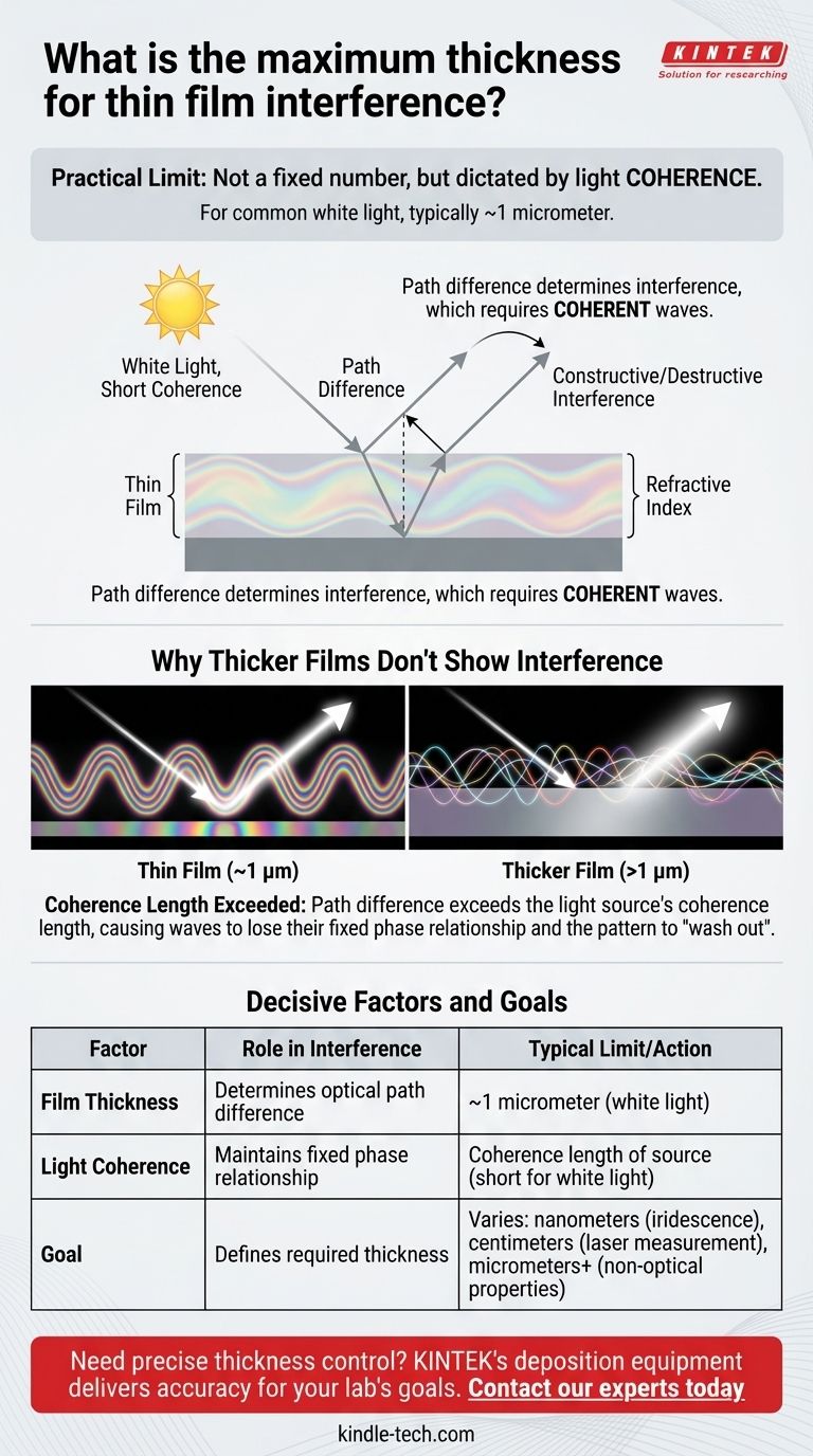
The maximum thickness for observable thin film interference is not a fixed number, but a practical limit dictated by the coherence of the light source. For common white light, this limit is typically around one micrometer, because at greater thicknesses, the reflected light waves lose their fixed phase relationship and the interference pattern washes out.
The Principle of Thin Film Interference
To understand the thickness limit, we first need to understand the mechanism that creates the effect. Interference is the result of light waves interacting with each other.
How Light Waves Interact in a Film
When light strikes a thin film, such as a soap bubble or an oil slick, some of it reflects off the top surface. The rest of the light enters the film, reflects off the bottom surface, and travels back out.
You now have two separate light waves traveling in the same direction. Thin film interference is what happens when these two waves meet and combine.
The Critical Role of Path Difference
The wave that travels through the film covers a longer distance than the wave that reflects from the top surface. This extra distance is called the optical path difference.
The path difference is determined primarily by the film's thickness and its refractive index. It is this difference that dictates whether the waves will reinforce each other (constructive interference, creating bright color) or cancel each other out (destructive interference, creating dark bands).
The Concept of Coherence
For interference to occur, the two reflected waves must be coherent. This means they must originate from the same initial wave and maintain a constant, predictable phase relationship with each other.
Think of it like two dancers trying to perform a synchronized routine. If they start in sync and stay in sync, their combined movements are structured and powerful. If one dancer is delayed, they fall out of sync, and the routine becomes a chaotic mess.
Why Thicker Films Don't Show Interference
The limit on thin film interference is fundamentally a limit of coherence. As the film gets thicker, the two reflected waves can no longer maintain their synchronized "dance."
Exceeding the Coherence Length
Every light source has a property called coherence length. This is the maximum path difference over which its light waves can maintain a fixed phase relationship.
Natural light sources like the sun or a lightbulb are a jumble of countless independent waves. They have a very short coherence length, typically less than a micrometer.
If a film is so thick that the path difference it creates exceeds the light's coherence length, the two reflected waves become effectively unrelated.
The "Washing Out" Effect
When the reflected waves are no longer coherent, they still combine, but their phase relationship is random. The constructive and destructive effects average out over the entire spectrum.
Instead of seeing distinct colors or patterns, our eyes perceive a uniform reflection. The interference fringes become so numerous and tightly packed that they blur together, effectively "washing out" into white light.
Understanding the Nuances
The term "maximum thickness" can be misleading because it depends on context. It's crucial to distinguish between the general definition of a thin film and the specific requirements for interference.
"Thin Film" vs. The Interference Limit
For material science and deposition, a film up to 100 micrometers thick may still be considered a "thin film." However, it is far too thick to produce visible interference patterns with a normal light source.
The "one micrometer" rule of thumb applies specifically to the optical phenomenon of interference with white light.
The Light Source Is a Decisive Factor
The breakdown of interference is a function of the light source's coherence length. A highly coherent light source, like a laser, has a coherence length that can be meters or even kilometers long.
With a laser, you can create and measure interference patterns in materials that are centimeters thick or more. This is the principle behind many high-precision interferometers used in science and engineering.
Applying This to Your Goal
The ideal film thickness is entirely dependent on what you are trying to achieve.
- If your primary focus is creating visible iridescence (e.g., decorative coatings, soap bubbles): Keep the film thickness within the range of a few hundred nanometers to about one micrometer to work well with white light.
- If your primary focus is precision measurement using interferometry: The maximum thickness is limited only by the coherence length of your light source, allowing for much thicker samples if you use a laser.
- If your primary focus is non-optical properties (e.g., electrical conductivity, material strength): The film's thickness can be much greater, but you should not expect to see classic interference effects at thicknesses beyond a few micrometers.
Ultimately, observing thin film interference is a delicate interplay between the thickness of the film and the coherence of the light illuminating it.
Summary Table:
| Factor | Role in Thin Film Interference | Typical Limit for Visible Interference |
|---|---|---|
| Film Thickness | Determines the optical path difference between reflected waves. | ~1 micrometer (for white light) |
| Light Coherence | Dictates if waves maintain a fixed phase relationship for interference. | Coherence length of the source (short for white light) |
| Goal | Defines the required thickness (e.g., iridescence vs. measurement). | Varies (nanometers for color, centimeters with lasers) |
Need to precisely control film thickness for your application? Whether you're developing decorative coatings, optical sensors, or advanced materials, KINTEK's range of deposition equipment and consumables delivers the accuracy and repeatability your lab requires. Contact our experts today to discuss how we can support your thin film research and production goals.
Visual Guide