Knowledge What is the nature of thin film? Unlocking Engineered Functionality at the Atomic Scale
Author avatar

Tech Team · Kintek Solution

Updated 1 day ago

What is the nature of thin film? Unlocking Engineered Functionality at the Atomic Scale

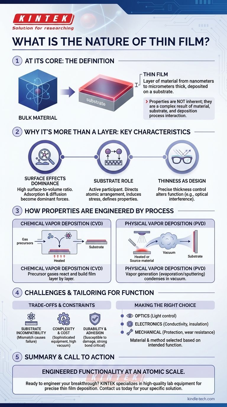
At its core, a thin film is a layer of material with a thickness ranging from just a few atoms (nanometers) to several micrometers, deposited onto a supporting surface known as a substrate. While defined by its minimal thickness, its true nature lies in how this dimension fundamentally alters its properties, making it behave very differently from the same material in its bulk form.

The defining characteristic of a thin film is not just its thinness. It is the fact that its properties are no longer inherent to the material alone, but are instead a complex result of the interaction between the material, the underlying substrate, and the precise method used for its deposition.

Why a Thin Film is More Than Just a Thin Layer

A block of gold and a thin film of gold are both made of gold atoms, but they do not behave the same way. The film's properties are dominated by its geometry and its environment, creating a unique material class.

The Dominance of Surface Effects

In a bulk material, most atoms are surrounded by other atoms. In a thin film, a huge proportion of atoms are at a surface or an interface.

This high surface-area-to-volume ratio means that surface phenomena—such as the adsorption of molecules from the environment or the diffusion (movement) of atoms across the surface—become dominant forces that dictate the film's behavior and stability.

The Critical Role of the Substrate

The substrate is not merely a passive holder for the film; it is an active participant in its structure.

The atomic arrangement, thermal expansion, and even the cleanliness of the substrate surface can direct how the film's atoms arrange themselves. This can induce stress, change the film's crystal structure, and ultimately define its electronic or optical properties.

Thickness as a Design Parameter

In the world of thin films, thickness is a powerful design tool. Changing the thickness by just a few nanometers can completely alter a film's function.

For example, this is how anti-reflection coatings on eyeglasses work. The thickness is precisely tuned to cause destructive interference for specific wavelengths of light, making the lens more transparent.

How Properties are Engineered by Process

A thin film's final characteristics are not an accident; they are a direct result of a highly controlled manufacturing process. The "how" it's made is just as important as the "what" it's made of.

The Blueprint: Deposition Methods

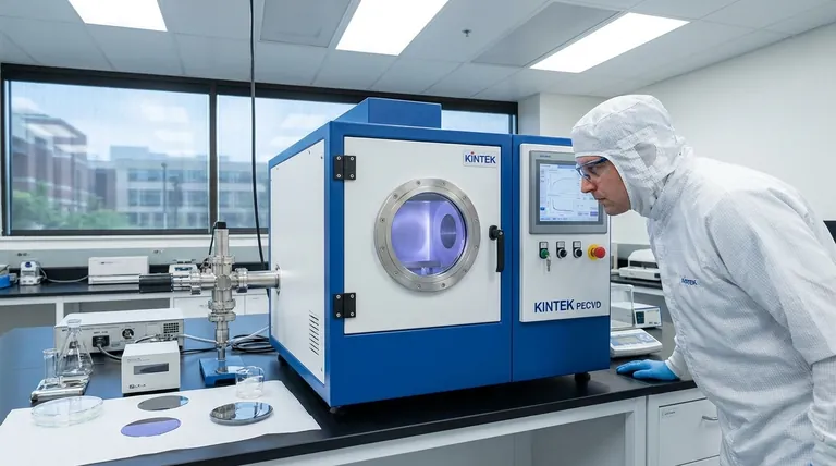
The process of creating a thin film is called deposition. The two most common families of techniques are Chemical Vapor Deposition (CVD) and Physical Vapor Deposition (PVD).

  • CVD uses precursor gases that react and decompose on the substrate surface to build the film layer by layer, almost like constructing it from atomic building blocks.
  • PVD involves generating a vapor of the source material—either by heating it (evaporation) or bombarding it with ions (sputtering)—which then travels through a vacuum and condenses onto the substrate.

Other specialized techniques like ion implantation and plasma etching are used to further modify these layers.

Tailoring for Specific Functions

By precisely controlling deposition parameters—such as temperature, pressure, and deposition rate—engineers can fine-tune a film's properties.

This control allows for the creation of films that are transparent, scratch-resistant, electrically conductive, insulating, or that selectively transmit signals, all based on the needs of the application.

Understanding the Trade-offs and Constraints

The highly engineered nature of thin films also introduces specific challenges. Understanding these limitations is critical for their successful application.

Substrate Incompatibility

Not every material can be effectively deposited on every substrate. A mismatch in crystal structure or thermal properties can lead to high internal stress, causing the film to crack, peel, or fail to adhere properly (delamination).

Process Complexity and Cost

Creating high-quality thin films requires sophisticated and expensive equipment operating in highly controlled environments, often under high vacuum. This makes the process significantly more complex and costly than working with bulk materials.

Durability and Adhesion

Because they are so thin, films can be susceptible to mechanical damage. Strong adhesion to the substrate is paramount for durability, and ensuring this bond is a primary engineering challenge in nearly every application.

Making the Right Choice for Your Goal

The selection of a thin film's material and deposition method is always driven by the intended function.

  • If your primary focus is optics or photonics: You will manipulate film thickness and material refractive index to precisely control how light reflects, absorbs, or transmits.
  • If your primary focus is electronics: You will select materials and deposition methods to achieve exact levels of electrical conductivity, insulation, or semiconducting behavior for creating circuits.
  • If your primary focus is mechanical protection: You will prioritize deposition processes that create dense, hard, and strongly adhered layers for scratch, wear, and corrosion resistance.

Ultimately, the nature of a thin film is one of controlled, engineered functionality at an atomic scale.

Summary Table:

Aspect Key Takeaway
Definition A layer of material, from nanometers to micrometers thick, deposited on a substrate.
Core Nature Properties are not inherent but engineered through interaction with the substrate and deposition process.
Key Effects Dominated by surface effects, substrate influence, and precise thickness control.
Primary Methods Chemical Vapor Deposition (CVD) and Physical Vapor Deposition (PVD).
Common Applications Optical coatings, electronic circuits, and protective mechanical layers.

Ready to engineer your next breakthrough with precision thin films?

The nature of thin film technology is complex, but achieving the perfect deposition for your specific application doesn't have to be. KINTEK specializes in high-quality lab equipment and consumables for thin film deposition, serving the precise needs of research and industrial laboratories.

We provide the reliable tools and expert support you need to master surface effects, ensure strong adhesion, and tailor properties for optics, electronics, or mechanical protection. Let us help you turn material science into real-world innovation.

Contact KINTEK today to discuss your project and discover the right solution for your laboratory.

Related Products

People Also Ask

Related Products

Inclined Rotary Plasma Enhanced Chemical Vapor Deposition PECVD Equipment Tube Furnace Machine

Inclined Rotary Plasma Enhanced Chemical Vapor Deposition PECVD Equipment Tube Furnace Machine

Upgrade your coating process with PECVD coating equipment. Ideal for LED, power semiconductors, MEMS and more. Deposits high-quality solid films at low temps.

Electron Beam Evaporation Coating Oxygen-Free Copper Crucible and Evaporation Boat

Electron Beam Evaporation Coating Oxygen-Free Copper Crucible and Evaporation Boat

Electron Beam Evaporation Coating Oxygen-Free Copper Crucible enables precise co-deposition of various materials. Its controlled temperature and water-cooled design ensure pure and efficient thin film deposition.

Custom CVD Diamond Coating for Lab Applications

Custom CVD Diamond Coating for Lab Applications

CVD Diamond Coating: Superior Thermal Conductivity, Crystal Quality, and Adhesion for Cutting Tools, Friction, and Acoustic Applications

Vacuum Hot Press Furnace Machine for Lamination and Heating

Vacuum Hot Press Furnace Machine for Lamination and Heating

Experience clean and precise lamination with Vacuum Lamination Press. Perfect for wafer bonding, thin-film transformations, and LCP lamination. Order now!

Microwave Plasma Chemical Vapor Deposition MPCVD Machine System Reactor for Lab and Diamond Growth

Microwave Plasma Chemical Vapor Deposition MPCVD Machine System Reactor for Lab and Diamond Growth

Get high-quality diamond films with our Bell-jar Resonator MPCVD machine designed for lab and diamond growth. Discover how Microwave Plasma Chemical Vapor Deposition works for growing diamonds using carbon gas and plasma.

Customer Made Versatile CVD Tube Furnace Chemical Vapor Deposition Chamber System Equipment

Customer Made Versatile CVD Tube Furnace Chemical Vapor Deposition Chamber System Equipment

Get your exclusive CVD furnace with KT-CTF16 Customer Made Versatile Furnace. Customizable sliding, rotating, and tilting functions for precise reactions. Order now!

Custom PTFE Teflon Parts Manufacturer for Hydrothermal Synthesis Reactor Polytetrafluoroethylene Carbon Paper and Carbon Cloth Nano-growth

Custom PTFE Teflon Parts Manufacturer for Hydrothermal Synthesis Reactor Polytetrafluoroethylene Carbon Paper and Carbon Cloth Nano-growth

Acid and alkali resistant polytetrafluoroethylene experimental fixtures meet different requirements. The material is made of brand new polytetrafluoroethylene material, which has excellent chemical stability, corrosion resistance, airtightness, high lubricity and non-stickiness, electrical corrosion and good anti-aging ability, and can work for a long time at temperatures from -180℃ to +250℃.

Cylindrical Resonator MPCVD Machine System Reactor for Microwave Plasma Chemical Vapor Deposition and Lab Diamond Growth

Cylindrical Resonator MPCVD Machine System Reactor for Microwave Plasma Chemical Vapor Deposition and Lab Diamond Growth

Learn about Cylindrical Resonator MPCVD Machine, the microwave plasma chemical vapor deposition method used for growing diamond gemstones and films in the jewelry and semi-conductor industries. Discover its cost-effective advantages over traditional HPHT methods.

Ultra-Vacuum Electrode Feedthrough Connector Flange Power Electrode Lead for High-Precision Applications

Ultra-Vacuum Electrode Feedthrough Connector Flange Power Electrode Lead for High-Precision Applications

Discover the Ultra-Vacuum Electrode Feedthrough Connector Flange, perfect for high-precision applications. Ensure reliable connections in ultra-vacuum environments with advanced sealing and conductive technology.

Custom PTFE Teflon Parts Manufacturer for Non-Standard Insulator Customization

Custom PTFE Teflon Parts Manufacturer for Non-Standard Insulator Customization

PTFE insulator PTFE has excellent electrical insulation properties in a wide temperature and frequency range.

Optical Ultra-Clear Glass Sheet for Laboratory K9 B270 BK7

Optical Ultra-Clear Glass Sheet for Laboratory K9 B270 BK7

Optical glass, while sharing many characteristics with other types of glass, is manufactured using specific chemicals that enhance properties crucial for optics applications.

Custom PTFE Teflon Parts Manufacturer Corrosion Resistant Cleaning Rack Flower Basket

Custom PTFE Teflon Parts Manufacturer Corrosion Resistant Cleaning Rack Flower Basket

The PTFE cleaning rack, also known as the PTFE flower basket cleaning flower basket, is a specialized laboratory tool designed for the efficient cleaning of PTFE materials. This cleaning rack ensures thorough and safe cleaning of PTFE items, maintaining their integrity and performance in laboratory settings.

Laboratory Vortex Mixer Orbital Shaker Multifunctional Rotation Oscillation Mixer

Laboratory Vortex Mixer Orbital Shaker Multifunctional Rotation Oscillation Mixer

The inching mixer is small in size, mixes quickly and thoroughly, and the liquid is in a vortex shape, which can mix all the test solutions attached to the tube wall.

Single Punch Electric Tablet Press Machine Laboratory Powder Tablet Punching TDP Tablet Press

Single Punch Electric Tablet Press Machine Laboratory Powder Tablet Punching TDP Tablet Press

The single-punch electric tablet press is a laboratory-scale tablet press suitable for corporate laboratories in pharmaceutical, chemical, food, metallurgical and other industries.

Vacuum Heat Treat and Pressure Sintering Furnace for High Temperature Applications

Vacuum Heat Treat and Pressure Sintering Furnace for High Temperature Applications

Vacuum pressure sintering furnaces are designed for high temperature hot pressing applications in metal and ceramic sintering. Its advanced features ensure precise temperature control, reliable pressure maintenance, and a robust design for seamless operation.

Graphite Vacuum Furnace Bottom Discharge Graphitization Furnace for Carbon Materials

Graphite Vacuum Furnace Bottom Discharge Graphitization Furnace for Carbon Materials

Bottom-out graphitization furnace for carbon materials, ultra-high temperature furnace up to 3100°C, suitable for graphitization and sintering of carbon rods and carbon blocks. Vertical design, bottom discharging, convenient feeding and discharging, high temperature uniformity, low energy consumption, good stability, hydraulic lifting system, convenient loading and unloading.

Custom PTFE Teflon Parts Manufacturer for Culture Dish and Evaporation Dish

Custom PTFE Teflon Parts Manufacturer for Culture Dish and Evaporation Dish

The PTFE culture dish evaporating dish is a versatile laboratory tool known for its chemical resistance and high-temperature stability. PTFE, a fluoropolymer, offers exceptional non-stick properties and durability, making it ideal for various applications in research and industry, including filtration, pyrolysis, and membrane technology.

600T Vacuum Induction Hot Press Furnace for Heat Treat and Sintering

600T Vacuum Induction Hot Press Furnace for Heat Treat and Sintering

Discover the 600T Vacuum Induction Hot Press Furnace, designed for high-temperature sintering experiments in vacuum or protected atmospheres. Its precise temperature and pressure control, adjustable working pressure, and advanced safety features make it ideal for nonmetal materials, carbon composites, ceramics, and metal powders.

Custom PTFE Teflon Parts Manufacturer for Hollow Etching Flower Basket ITO FTO Developing Glue Removal

Custom PTFE Teflon Parts Manufacturer for Hollow Etching Flower Basket ITO FTO Developing Glue Removal

PTFE adjustable height flower basket (Teflon flower baskets) are made of high-purity experimental grade PTFE, with excellent chemical stability, corrosion resistance, sealing and high and low temperature resistance.

High Shear Homogenizer for Pharmaceutical and Cosmetic Applications

High Shear Homogenizer for Pharmaceutical and Cosmetic Applications

Enhance lab efficiency with our high-speed Laboratory Emulsifier Homogenizer for precise, stable sample processing. Ideal for pharmaceuticals & cosmetics.


Leave Your Message