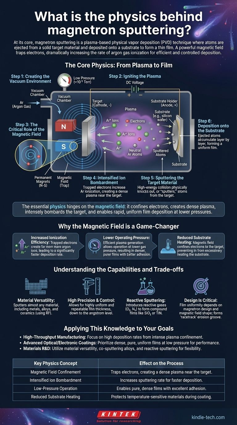
At its core, magnetron sputtering is a plasma-based physical vapor deposition (PVD) technique where atoms are ejected from a solid target material and deposited onto a substrate to form a thin film. The process begins by creating a plasma from an inert gas, like argon. A powerful magnetic field is then used to trap electrons near the target, dramatically increasing the rate at which the argon gas is ionized, leading to a much more efficient and controlled deposition process.
The essential physics of magnetron sputtering hinges on one critical component: the magnetic field. By confining electrons near the target surface, the magnetron creates a dense, stable plasma that intensely bombards the target, enabling rapid and uniform film deposition at lower pressures than other sputtering methods.
The Core Physics: From Plasma to Film
To understand magnetron sputtering, it's best to break it down into a sequence of physical events. Each step builds upon the last, culminating in the creation of a high-quality thin film.
Step 1: Creating the Vacuum Environment
The entire process occurs within a vacuum chamber. Air is pumped out, and an inert gas, most commonly argon (Ar), is introduced at a very low, controlled pressure.
This low-pressure environment is critical because it ensures the sputtered atoms can travel from the target to the substrate with minimal collisions with other gas molecules.
Step 2: Igniting the Plasma
A high DC voltage is applied between two electrodes. The material to be deposited, known as the target, is mounted on the negative electrode (the cathode). The substrate holder or chamber walls act as the positive electrode (the anode).
This strong electric field energizes the argon gas, stripping electrons from some argon atoms. This creates a mixture of positively charged argon ions (Ar+), free electrons (e⁻), and neutral argon atoms, which we call a plasma.
Step 3: The Critical Role of the Magnetic Field
This is the "magnetron" part of the name. A set of strong permanent magnets is placed behind the target. These magnets generate a magnetic field that emerges from the face of the target and loops back around.
This magnetic field is perpendicular to the electric field in a specific region near the target surface. Its sole purpose is to trap the free electrons and force them to move in a spiral path close to the target.
Step 4: Intensified Ion Bombardment
Without the magnetic field, electrons would quickly fly to the anode. By trapping them, the magnetic field dramatically increases the path length of each electron.
As these electrons spiral, their chances of colliding with and ionizing neutral argon atoms increase exponentially. This creates a dense, self-sustaining plasma concentrated directly in front of the target.
Step 5: Sputtering the Target Material
The negatively charged target strongly attracts the abundant, positively charged argon ions from this dense plasma.
These ions accelerate toward the target, striking its surface with significant kinetic energy. This high-energy collision physically knocks out, or "sputters," atoms from the target material.
Step 6: Deposition onto the Substrate
The ejected atoms from the target travel through the low-pressure chamber and land on the surface of the substrate (e.g., a silicon wafer, glass, or metal part).
As these atoms accumulate, they build up layer by layer, forming a thin, uniform, and often very dense film.
Why the Magnetic Field is a Game-Changer
The addition of the magnetic field is what elevates magnetron sputtering above simpler diode sputtering methods. The benefits are a direct consequence of the physics of electron confinement.
Increased Ionization Efficiency
The trapped electrons create far more argon ions than would otherwise be possible. This high ion density leads to a much higher rate of ion bombardment, resulting in a significantly faster deposition rate.
Lower Operating Pressure
Because the plasma is so efficiently generated and sustained near the target, the system can operate at a much lower gas pressure.
Lower pressure means fewer gas-phase collisions for the sputtered atoms as they travel to the substrate. This results in films that are denser, purer, and have better adhesion.
Reduced Substrate Heating
The magnetic field confines the high-energy electrons to the target area, preventing them from bombarding and excessively heating the substrate. This is crucial when coating temperature-sensitive materials like plastics or complex electronic devices.
Understanding the Capabilities and Trade-offs
The physics of the process enables a unique set of advantages but also requires careful engineering.
Material Versatility
The sputtering process is a physical momentum transfer, not a chemical or thermal one. This means almost any material can be sputtered, including metals, alloys, and even ceramic or insulating materials (which requires a variation using RF power).
High Precision and Control
By carefully controlling parameters like gas pressure, voltage, and time, magnetron sputtering allows for the deposition of films with highly uniform and repeatable thickness, often controlled down to the angstrom level.
Reactive Sputtering for Compounds
A reactive gas like oxygen or nitrogen can be introduced along with the argon. When sputtered metal atoms travel to the substrate, they react with this gas to form compound films like oxides (e.g., SiO₂) or nitrides (e.g., TiN).
Design Is Critical
The uniformity of the deposited film is heavily dependent on the design of the magnetron, specifically the strength and shape of the magnetic field. The "racetrack," or erosion groove, that forms on the target is a direct visualization of the region of most intense plasma confinement.
Applying This Knowledge to Your Goals
Your specific application will determine which aspect of magnetron sputtering physics is most important to you.
- If your primary focus is high-throughput manufacturing: The high deposition rates enabled by intense plasma confinement are your key advantage for industrial-scale production.
- If your primary focus is advanced optical or electronic coatings: The dense, pure, and uniform films produced at low pressure are critical for achieving desired performance and reliability.
- If your primary focus is materials research and development: The ability to co-sputter alloys, create compounds with reactive sputtering, and precisely control film structure offers unmatched flexibility.
Ultimately, the physics of magnetron sputtering reveals a brilliantly engineered process that uses electric and magnetic fields to create a uniquely effective tool for thin-film deposition.
Summary Table:
| Key Physics Concept | Effect on the Process |
|---|---|
| Magnetic Field Confinement | Traps electrons, creating a dense plasma near the target. |
| Intensified Ion Bombardment | Increases sputtering rate for faster deposition. |
| Low-Pressure Operation | Enables pure, dense films with excellent adhesion. |
| Reduced Substrate Heating | Protects temperature-sensitive materials during coating. |
Ready to leverage the precision of magnetron sputtering in your lab? KINTEK specializes in high-performance lab equipment and consumables for all your thin-film deposition needs. Whether you are in R&D or high-throughput manufacturing, our solutions deliver the uniform, high-quality coatings essential for advanced optics, electronics, and materials science. Contact our experts today to discuss how we can optimize your PVD process!
Visual Guide
Related Products
- Microwave Plasma Chemical Vapor Deposition MPCVD Machine System Reactor for Lab and Diamond Growth
- Chemical Vapor Deposition CVD Equipment System Chamber Slide PECVD Tube Furnace with Liquid Gasifier PECVD Machine
- Molybdenum Tungsten Tantalum Special Shape Evaporation Boat
- Inclined Rotary Plasma Enhanced Chemical Vapor Deposition PECVD Equipment Tube Furnace Machine
- Inclined Rotary Plasma Enhanced Chemical Vapor Deposition PECVD Equipment Tube Furnace Machine
People Also Ask
- What are the advantages of a Microwave Plasma CVD reactor for MCD/NCD coatings? Precision Multilayer Diamond Engineering
- How does a microwave plasma reactor facilitate the synthesis of diamond? Master MPCVD with Precision Technology
- What pressure is needed for chemical vapor deposition of diamonds? Master the Low-Pressure 'Sweet Spot'
- How are CVD diamonds created? Discover the Science of Lab-Grown Diamond Precision
- How do vacuum pumps and valves collaborate in MPCVD? Achieve Precise Pressure Control for Superior CNT Synthesis