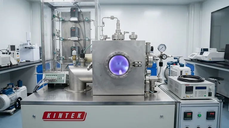
In essence, plasma layer deposition is a high-performance coating process that uses an energized, ionized gas—known as plasma—to create exceptionally thin and durable films on a material's surface. This process occurs within a vacuum chamber, where precursor materials are broken down into their fundamental components and reassembled onto a substrate, atom by atom, to enhance properties like hardness, corrosion resistance, or electrical conductivity.
The core principle is not simply applying a layer of material, but fundamentally changing a surface by constructing a new, highly-engineered film from atomic or molecular building blocks generated within a high-energy plasma environment.
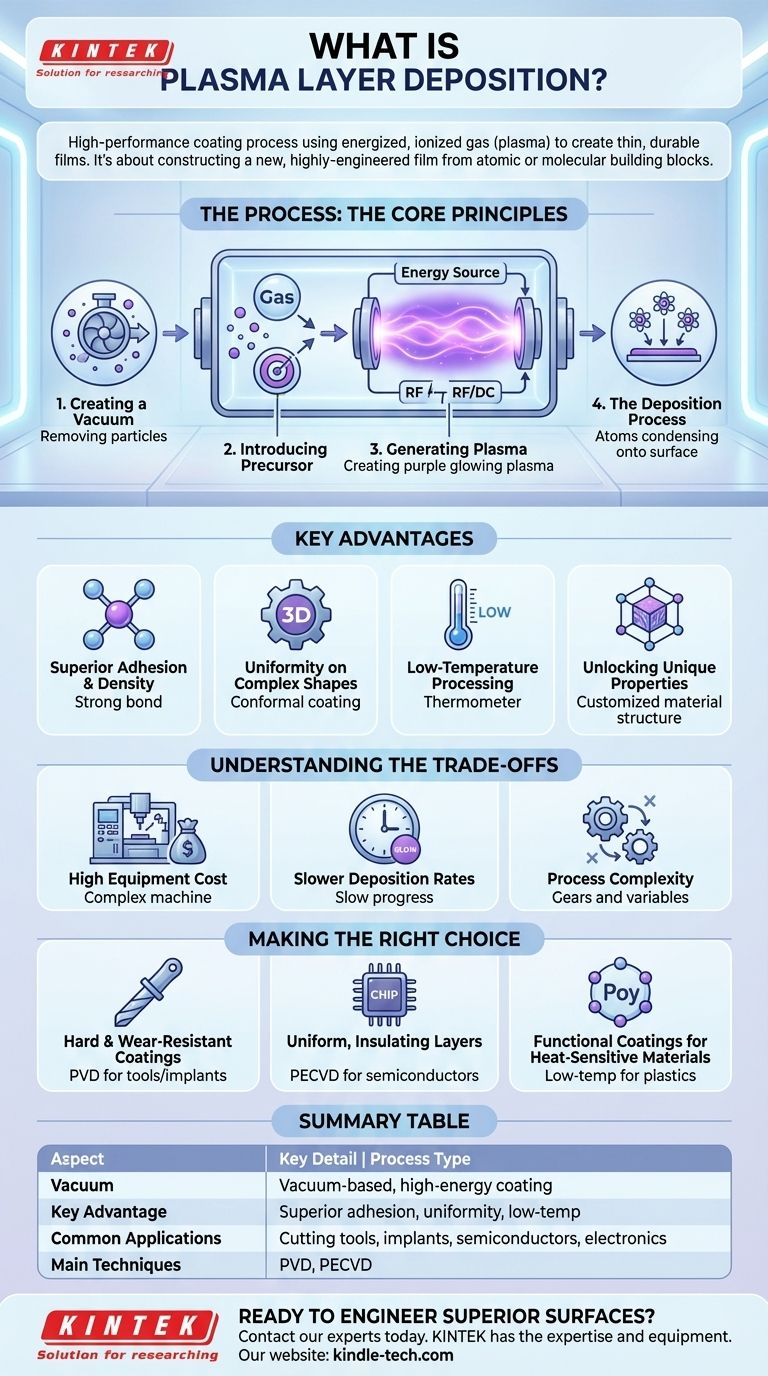
How Plasma Deposition Works: The Core Principles
To understand plasma deposition, it's best to break it down into the distinct stages that occur inside a specialized vacuum chamber.
Step 1: Creating a Vacuum
Before any coating can begin, the chamber is evacuated to an extremely low pressure. This is critical for removing air, water vapor, and other contaminants that would otherwise interfere with the process and compromise the quality of the final layer.
Step 2: Introducing the Precursor Material
The material intended for the coating is introduced into the chamber. Depending on the specific technique, this could be a gas (for chemical vapor deposition) or a solid "target" that will be physically bombarded (for physical vapor deposition).
Step 3: Generating the Plasma
A powerful energy source, such as a radio frequency (RF) or direct current (DC) electrical field, is applied to the chamber. This energy strips electrons from the atoms of the precursor gas, creating a glowing, highly reactive mix of ions, electrons, and neutral particles known as plasma, often called the fourth state of matter.
Step 4: The Deposition Process
The highly energetic species within the plasma are then directed toward the object being coated (the substrate). They condense on its surface, forming a thin, dense, and highly uniform film. Because the particles have such high energy, they create a layer with superior adhesion and structural integrity compared to conventional coating methods.
Key Advantages of Using Plasma
Plasma deposition is not chosen for its simplicity, but for the unparalleled results it delivers in demanding applications.
Superior Adhesion and Density
The high kinetic energy of the plasma particles embeds them slightly into the substrate surface, creating an exceptionally strong bond. This energy also ensures the deposited atoms are tightly packed, resulting in a dense, non-porous coating.
Uniformity on Complex Shapes
Unlike line-of-sight methods like paint spraying, the plasma fills the entire chamber. This allows it to deposit a perfectly uniform, or conformal, coating over complex, three-dimensional shapes without thin spots or gaps.
Low-Temperature Processing
Many plasma deposition techniques can be performed at relatively low temperatures. This is a crucial advantage when coating heat-sensitive materials like polymers or certain electronics that would be damaged or destroyed by high-heat thermal processes.
Unlocking Unique Material Properties
The plasma environment can create coatings with unique chemical structures and properties that are impossible to achieve through other means. This allows for the engineering of materials with tailored optical, electrical, or mechanical characteristics.
Understanding the Trade-offs
While powerful, plasma deposition is a specialized process with specific limitations that make it unsuitable for certain applications.
High Equipment Cost
Plasma deposition systems require sophisticated and expensive equipment, including vacuum chambers, high-power energy sources, and precise gas flow controllers. This represents a significant capital investment.
Slower Deposition Rates
Building a coating layer by layer at the atomic level is an inherently slow process. For applications requiring very thick coatings, the time required can be prohibitively long compared to methods like thermal spraying or electroplating.
Process Complexity
The quality of the final coating is extremely sensitive to process variables like pressure, gas composition, temperature, and power levels. It requires significant expertise to develop and maintain a stable, repeatable process.
Making the Right Choice for Your Goal
Selecting a coating technology depends entirely on the intended application and performance requirements.
- If your primary focus is creating extremely hard, wear-resistant coatings for cutting tools or medical implants: Physical Vapor Deposition (PVD), a type of plasma deposition, is the industry standard for materials like Titanium Nitride (TiN).
- If your primary focus is depositing uniform, electrically insulating layers in semiconductor manufacturing: Plasma-Enhanced Chemical Vapor Deposition (PECVD) is essential for creating the high-purity silicon dioxide and silicon nitride films that form the backbone of modern electronics.
- If your primary focus is adding a functional coating to heat-sensitive plastics or polymers: The low-temperature capabilities of plasma deposition make it one of the few viable options for enhancing the surface of these materials without causing thermal damage.
Ultimately, plasma deposition is a powerful tool of materials science, enabling the creation of surfaces with properties far beyond what the bulk material alone can offer.
Summary Table:
| Aspect | Key Detail |
|---|---|
| Process Type | Vacuum-based, high-energy coating |
| Key Advantage | Superior adhesion, uniformity, and low-temperature processing |
| Common Applications | Cutting tools, medical implants, semiconductors, electronics |
| Main Techniques | PVD (Physical Vapor Deposition), PECVD (Plasma-Enhanced Chemical Vapor Deposition) |
Ready to Engineer Superior Surfaces?
Plasma deposition technology can unlock new levels of performance for your products. Whether you need wear-resistant coatings for tools, functional layers for electronics, or protective films for sensitive materials, KINTEK has the expertise and equipment to meet your specific laboratory needs.
Contact our experts today to discuss how our plasma deposition solutions can enhance your materials and give you a competitive edge.
Visual Guide