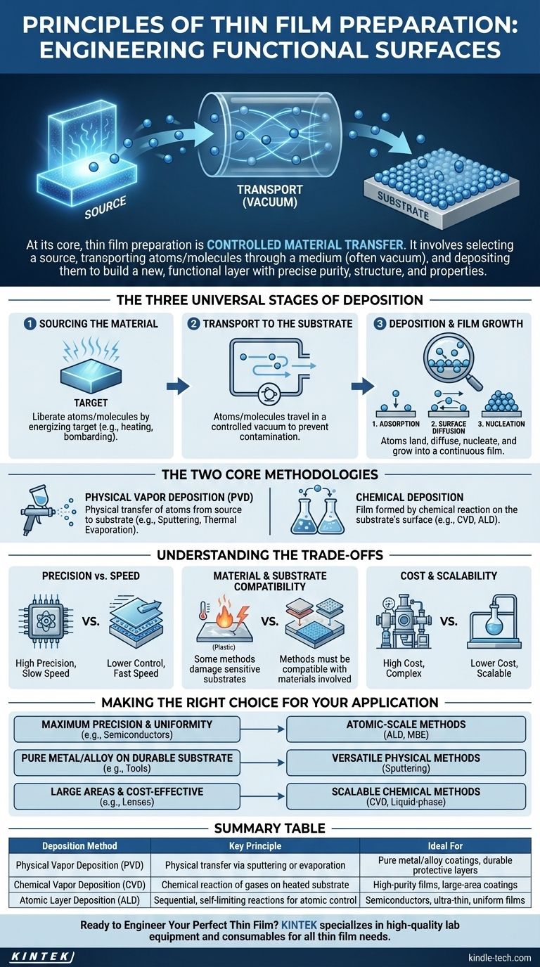
At its core, the principle of thin film preparation is a process of controlled material transfer. It involves three fundamental steps: selecting a source material (the target), transporting its atoms or molecules through a medium, and depositing them onto a surface (the substrate) to build a new, functional layer. This entire process is meticulously managed, often within a vacuum, to ensure the resulting film has the precise purity, structure, and properties required for its application.
The fundamental goal of thin film preparation is not just to add a layer, but to engineer a new surface with specific, enhanced properties. The process hinges on controlling the journey of individual atoms or molecules from a source to a substrate, where they self-organize into a functional film.
The Three Universal Stages of Deposition
Every thin film deposition technique, regardless of its complexity, follows a universal sequence of events. Understanding these stages is key to controlling the final outcome.
Stage 1: Sourcing the Material
The process begins with a source material, often called a target. This is the pure substance—be it a metal, oxide, or compound—that you intend to deposit. The first step is to liberate atoms or molecules from this source. This is achieved by energizing the target, for example, by heating it until it evaporates or by bombarding it with high-energy ions.
Stage 2: Transport to the Substrate
Once freed, these atoms or molecules must travel to the substrate. This transport phase almost always occurs in a highly controlled environment, such as a vacuum chamber. The vacuum prevents the traveling particles from colliding with and reacting to air molecules like oxygen or nitrogen, which would create impurities in the film.
Stage 3: Deposition and Film Growth
This is the most critical stage. When atoms arrive at the substrate, they don't simply stick in place. The process involves:
- Adsorption: The atom or molecule initially lands and weakly bonds to the surface.
- Surface Diffusion: The adsorbed atom uses its energy to move across the substrate's surface.
- Nucleation: Atoms find each other and cluster together, forming stable islands or "nuclei."
These nuclei then grow and merge, eventually forming a continuous thin film. The way this happens—the film's growth mode—is determined by the deposition conditions and dictates the film's final structure and properties.
The Two Core Methodologies: Physical vs. Chemical
While the stages are universal, the methods to achieve them fall into two major families. The choice between them depends entirely on the desired film characteristics, material, and application.
Physical Vapor Deposition (PVD)
In PVD, the material is physically transferred from the source to the substrate. Think of it as a microscopic form of spray painting, where individual atoms are the "paint."
Common PVD methods include sputtering, where an ion beam knocks atoms off a target, and thermal evaporation, where a material is heated in a vacuum until it vaporizes and condenses on the substrate. These methods are valued for their versatility and ability to deposit pure materials.
Chemical Deposition
In chemical methods, the film is not transferred directly but is instead formed by a chemical reaction on the substrate's surface. Precursor gases are introduced into a chamber, and when they react at the hot substrate surface, they form a solid material, leaving behind volatile byproducts.
Chemical Vapor Deposition (CVD) is a classic example. An even more precise technique is Atomic Layer Deposition (ALD), where precursors are pulsed in one at a time to build the film a single atomic layer at a time, offering unparalleled control over thickness and uniformity.
Understanding the Trade-offs
No single method is universally superior. The right choice involves balancing competing factors of control, cost, and material compatibility.
Precision vs. Speed
Methods like ALD offer atomic-level control, which is essential for manufacturing modern semiconductor chips where even a few misplaced atoms can cause device failure. However, this precision comes at the cost of speed. In contrast, methods like electroplating or thermal evaporation are much faster but offer less control over the film's structure.
Material and Substrate Compatibility
Some materials are difficult to vaporize and are better suited for sputtering (PVD). Other processes, like high-temperature CVD, can damage heat-sensitive substrates. The deposition method must be compatible with both the film material and the underlying substrate.
Cost and Scalability
High-vacuum systems used for techniques like Molecular Beam Epitaxy (MBE) are extremely expensive and complex. In contrast, chemical methods like sol-gel or dip coating can be performed with simpler equipment and are easily scaled up to coat large or irregularly shaped objects, making them ideal for industrial applications like anti-scratch coatings on glasses.
Making the Right Choice for Your Application
Your goal determines the optimal deposition strategy.
- If your primary focus is maximum precision and uniformity (e.g., semiconductors): You will need atomic-scale methods like Atomic Layer Deposition (ALD) or Molecular Beam Epitaxy (MBE).
- If your primary focus is depositing a pure metal or alloy onto a durable substrate (e.g., protective coatings on tools): A versatile physical method like sputtering is an excellent and widely used choice.
- If your primary focus is coating large areas or complex shapes cost-effectively (e.g., anti-reflective coatings on lenses): Scalable techniques like CVD or various liquid-phase chemical methods offer the best balance of performance and throughput.
Understanding these core principles empowers you to select not just a deposition technique, but the right path to engineering the exact material properties you need.
Summary Table:
| Deposition Method | Key Principle | Ideal For |
|---|---|---|
| Physical Vapor Deposition (PVD) | Physical transfer of atoms via sputtering or evaporation | Pure metal/alloy coatings, durable protective layers |
| Chemical Vapor Deposition (CVD) | Chemical reaction of gases on a heated substrate | High-purity films, large-area coatings |
| Atomic Layer Deposition (ALD) | Sequential, self-limiting reactions for atomic-level control | Semiconductors, ultra-thin, uniform films |
Ready to Engineer Your Perfect Thin Film?
Choosing the right deposition technique is critical for achieving the precise purity, structure, and performance your application demands. At KINTEK, we specialize in providing high-quality lab equipment and consumables for all your thin film preparation needs—from robust PVD sputtering systems to advanced ALD reactors.
Our experts can help you select the ideal solution to enhance your research or production process, ensuring superior film quality and efficiency. Contact us today to discuss your specific requirements and discover how KINTEK can support your laboratory's success.
Visual Guide