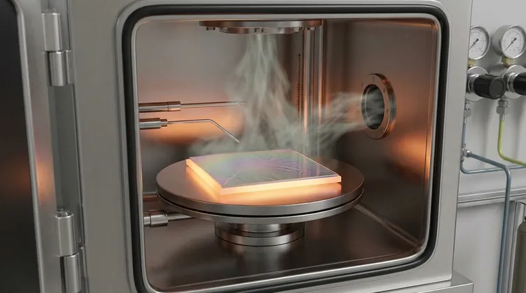
In essence, Chemical Vapor Deposition (CVD) is a process where volatile precursor gases are introduced into a reaction chamber where they decompose and react on a heated substrate surface. This chemical reaction results in the deposition of a high-quality, solid thin film on the substrate, while gaseous byproducts are removed.
At its core, Chemical Vapor Deposition is not just a coating method; it's a controlled chemical reaction on a surface. This chemical nature is the key to its ability to produce highly pure, dense, and uniform films on even the most complex shapes.
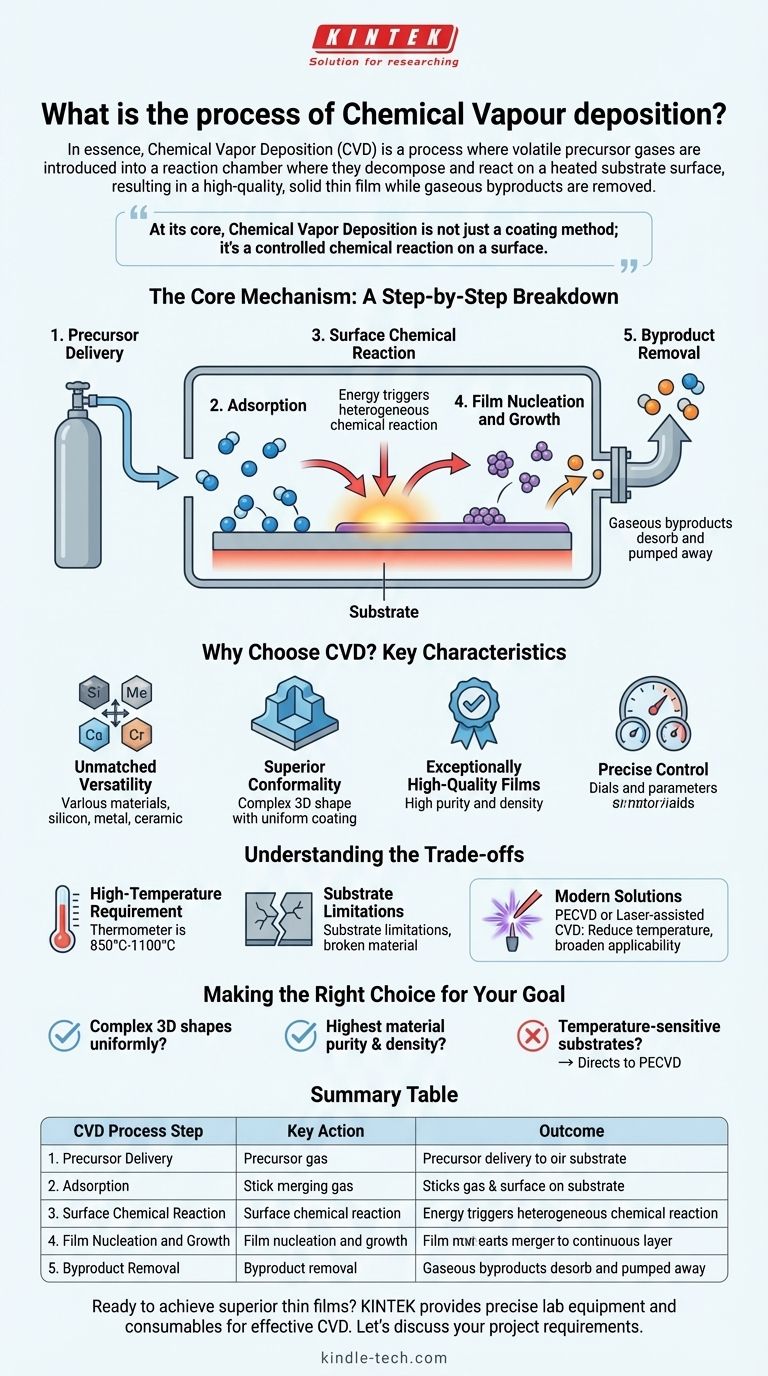
The Core Mechanism: A Step-by-Step Breakdown
To truly understand CVD, it's helpful to visualize the journey of the precursor molecules from a gas into a solid film. The entire process hinges on a series of carefully controlled physical and chemical events.
Step 1: Precursor Delivery
The process begins by transporting one or more reactive gases, known as precursors, into a deposition chamber. These precursors contain the elements that will ultimately form the final film.
Step 2: Adsorption on the Substrate
Once inside the chamber, the precursor gas molecules travel to the substrate—the material being coated. Here, they physically stick to the surface in a process called adsorption.
Step 3: The Surface Chemical Reaction
This is the heart of CVD. The energy provided by the heated substrate triggers a heterogeneous chemical reaction. The adsorbed precursor molecules either decompose or react with each other directly on the surface.
Step 4: Film Nucleation and Growth
The solid products from the chemical reaction begin to form stable clusters on the surface, a process called nucleation. These nuclei act as seeds, and as more atoms arrive and bond to them, they grow and merge to form a continuous, solid film.
Step 5: Byproduct Removal
The chemical reaction almost always creates gaseous byproducts that are not part of the desired film. These waste products desorb from the surface and are transported out of the reaction chamber by a continuous gas flow or vacuum system.
Why Choose CVD? Key Characteristics
The unique, reaction-based nature of CVD provides several distinct advantages that make it a critical process in industries from semiconductors to aerospace.
Unmatched Versatility
CVD can be used to deposit a vast range of materials. This includes metals, non-metals like silicon, and complex ceramic or compound layers like silicon carbide or titanium nitride.
Superior Conformality
Because the precursor is a gas, it can flow into and around intricate features. This gives CVD excellent "wrap-around" properties, allowing it to deposit a highly uniform film on complex 3D surfaces, something line-of-sight methods struggle with.
Exceptionally High-Quality Films
The films produced by CVD are known for their high purity and density. The process also tends to result in coatings with low residual stress and good crystalline structure.
Precise Control
By carefully adjusting deposition parameters—such as temperature, pressure, and gas flow rates—operators can precisely control the final film's chemical composition, crystal structure, and grain size.
Understanding the Trade-offs
No process is perfect. The primary limitation of traditional CVD is directly linked to the step that makes it so effective: the chemical reaction.
The High-Temperature Requirement
Most CVD processes require very high temperatures, typically between 850°C and 1100°C, to provide the necessary activation energy for the surface reactions to occur.
Substrate Limitations
This high heat requirement means that CVD cannot be used on many substrate materials, such as polymers or certain metals with low melting points, as they would be damaged or destroyed by the process.
Modern Solutions
To overcome this limitation, variants like Plasma-Enhanced CVD (PECVD) or laser-assisted CVD have been developed. These methods use plasma or laser energy to drive the chemical reaction, significantly reducing the required substrate temperature and broadening the range of applicable materials.
Making the Right Choice for Your Goal
Selecting a deposition technique depends entirely on the requirements of your application.
- If your primary focus is coating complex 3D shapes uniformly: CVD's gas-phase nature provides exceptional conformality that is difficult to achieve with line-of-sight methods.
- If your primary focus is achieving the highest material purity and density: The chemical reaction at the heart of CVD inherently produces films with very few impurities or structural voids.
- If your primary focus is working with temperature-sensitive substrates: Traditional high-temperature CVD is likely unsuitable, and you should investigate lower-temperature variants like PECVD.
Understanding the fundamental chemical nature of this process is the first step toward leveraging its power for advanced material fabrication.
Summary Table:
| CVD Process Step | Key Action | Outcome |
|---|---|---|
| 1. Precursor Delivery | Reactive gases are introduced into the chamber. | Precursors are available for reaction. |
| 2. Adsorption | Gas molecules stick to the heated substrate surface. | Precursors are in position for the chemical reaction. |
| 3. Surface Reaction | Heat energy triggers decomposition/reaction on the surface. | Solid film material is created from the gas precursors. |
| 4. Nucleation & Growth | Solid atoms form clusters that grow and merge. | A continuous, high-quality thin film is formed. |
| 5. Byproduct Removal | Gaseous waste products are desorbed and pumped away. | A pure film deposit is left on the substrate. |
Ready to achieve superior thin films for your laboratory?
The controlled chemical reactions of CVD are key to producing the high-purity, dense, and uniform coatings essential for advanced R&D and manufacturing. KINTEK specializes in providing the precise lab equipment and consumables needed to implement CVD and other deposition techniques effectively.
Let's discuss your project requirements. Contact our experts today to find the ideal solution for your specific substrate and material goals.
Visual Guide
Related Products
- Chemical Vapor Deposition CVD Equipment System Chamber Slide PECVD Tube Furnace with Liquid Gasifier PECVD Machine
- Microwave Plasma Chemical Vapor Deposition MPCVD Machine System Reactor for Lab and Diamond Growth
- 915MHz MPCVD Diamond Machine Microwave Plasma Chemical Vapor Deposition System Reactor
- Customer Made Versatile CVD Tube Furnace Chemical Vapor Deposition Chamber System Equipment
- Split Chamber CVD Tube Furnace with Vacuum Station Chemical Vapor Deposition System Equipment Machine
People Also Ask
- What happens during deposition chemistry? Building Thin Films from Gaseous Precursors
- What is plasma enhanced chemical vapor deposition PECVD equipment? A Guide to Low-Temperature Thin Film Deposition
- What are the processes of vapor phase deposition? Understand CVD vs. PVD for Superior Thin Films
- What are the advantages of chemical vapor deposition? Achieve Superior Thin Films for Your Lab
- How expensive is chemical vapor deposition? Understanding the True Cost of High-Performance Coating


