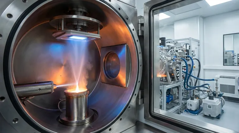
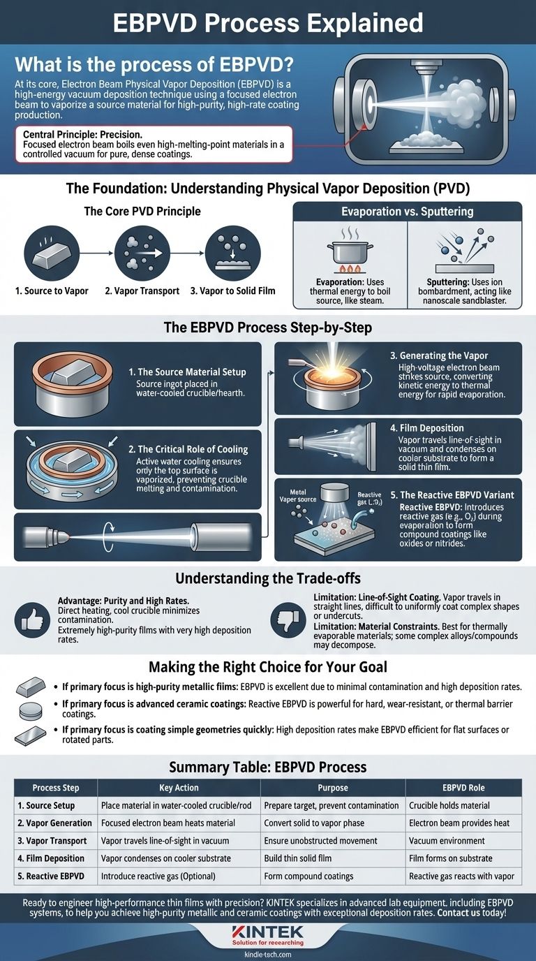
At its core, Electron Beam Physical Vapor Deposition (EBPVD) is a vacuum deposition technique where a high-energy beam of electrons is used to heat and vaporize a source material. This vapor then travels through the vacuum and condenses onto a cooler substrate, building a thin film or coating atom by atom. The entire process is valued for its ability to produce high-purity coatings at very high deposition rates.
The central principle of EBPVD is its precision. By using a focused electron beam as a heat source, it can boil even materials with very high melting points, allowing the resulting vapor to form exceptionally pure and dense coatings in a highly controlled vacuum environment.
The Foundation: Understanding Physical Vapor Deposition (PVD)
To grasp the specifics of EBPVD, it's essential to first understand the broader category of techniques it belongs to: Physical Vapor Deposition (PVD).
### The Core PVD Principle
All PVD processes share a fundamental, three-step sequence.
- A solid or liquid source material is converted into a vapor.
- This vapor is transported through a low-pressure (vacuum) environment.
- The vapor condenses on a target object (the substrate) to form a solid coating.
### Evaporation vs. Sputtering
PVD techniques are generally split into two families based on how they create the vapor. EBPVD is a form of evaporation, which uses thermal energy to boil the source material, much like boiling water creates steam.
The other family is sputtering, which uses energetic ion bombardment to physically knock atoms loose from the source material, acting like a nanoscale sandblaster.
The EBPVD Process Step-by-Step
The EBPVD method follows a precise workflow within a vacuum chamber to achieve its highly controlled results.
### The Source Material Setup
The starting material, often called an ingot, is placed in a water-cooled copper crucible or hearth. Alternatively, the material can be in the form of a rod mounted in a socket.
### The Critical Role of Cooling
The crucible or socket must be actively cooled, typically with circulating water. This is crucial because it ensures that only the top surface of the source material is vaporized by the electron beam, preventing the crucible itself from melting and contaminating the film.
### Generating the Vapor
A high-voltage power supply generates a focused beam of electrons. This beam is magnetically steered to strike the surface of the source material. The intense kinetic energy of the electrons is converted to thermal energy, rapidly heating the material past its boiling point and causing it to evaporate.
### Film Deposition
The resulting vapor of atoms or molecules travels in a straight, line-of-sight path through the vacuum chamber. When this vapor cloud reaches the relatively cool substrate, it condenses, forming a thin, solid film.
### The Reactive EBPVD Variant
For creating ceramic or compound films, a technique called reactive EBPVD is used. In this process, the metal is evaporated as usual, but a reactive gas (like oxygen for oxides or acetylene for carbides) is introduced into the chamber. The evaporated metal atoms react with the gas near the substrate to form the desired compound film.
Understanding the Trade-offs
Like any specialized process, EBPVD has distinct advantages and limitations that make it suitable for specific applications.
### Advantage: Purity and High Rates
Because the electron beam heats the source material directly and the crucible remains cool, there is very little contamination. This results in extremely high-purity films. The process can also achieve very high deposition rates compared to other methods.
### Limitation: Line-of-Sight Coating
The vapor travels in a straight line from the source to the substrate. This makes it difficult to uniformly coat complex shapes with undercuts or hidden surfaces without sophisticated substrate manipulation.
### Limitation: Material Constraints
The EBPVD process is best suited for materials that can be thermally evaporated without decomposing. Certain complex alloys or compounds may not be suitable for this technique.
Making the Right Choice for Your Goal
Selecting the right deposition method depends entirely on the desired outcome for your material or component.
- If your primary focus is high-purity metallic films: EBPVD is an excellent choice due to its direct heating method, which minimizes contamination and allows for high deposition rates.
- If your primary focus is advanced ceramic coatings: Reactive EBPVD provides a powerful method for creating hard, wear-resistant, or thermal barrier coatings like oxides and nitrides.
- If your primary focus is coating simple geometries quickly: EBPVD's high deposition rates make it highly efficient for coating relatively flat surfaces or parts that can be easily rotated to expose all faces to the vapor stream.
Ultimately, understanding the EBPVD process empowers you to select a highly controlled method for engineering advanced, high-performance thin films.
Summary Table:
| Process Step | Key Action | Purpose |
|---|---|---|
| 1. Source Setup | Place material in water-cooled crucible/rod | Prepare the target material for vaporization, preventing contamination |
| 2. Vapor Generation | Focused electron beam heats material to evaporate | Convert solid material into a vapor phase using precise thermal energy |
| 3. Vapor Transport | Vapor travels in line-of-sight through vacuum | Ensure atoms/molecules move without obstruction to the substrate |
| 4. Film Deposition | Vapor condenses on cooler substrate | Build a thin, solid film atom by atom onto the target surface |
| 5. Reactive EBPVD (Optional) | Introduce reactive gas (e.g., O₂, N₂) during evaporation | Form compound coatings like oxides or nitrides directly on the substrate |
Ready to engineer high-performance thin films with precision? KINTEK specializes in advanced lab equipment, including EBPVD systems, to help you achieve high-purity metallic and ceramic coatings with exceptional deposition rates. Whether you're developing wear-resistant surfaces, thermal barriers, or pure metallic films, our expertise ensures you get the right solution for your laboratory's unique needs. Contact us today to discuss how our EBPVD technology can accelerate your research and production goals!
Visual Guide
Related Products
- RF PECVD System Radio Frequency Plasma-Enhanced Chemical Vapor Deposition RF PECVD
- Chemical Vapor Deposition CVD Equipment System Chamber Slide PECVD Tube Furnace with Liquid Gasifier PECVD Machine
- Split Chamber CVD Tube Furnace with Vacuum Station Chemical Vapor Deposition System Equipment Machine
- Three-dimensional electromagnetic sieving instrument
- 1400℃ Controlled Atmosphere Furnace with Nitrogen and Inert Atmosphere
People Also Ask
- How are PECVD and CVD different? A Guide to Choosing the Right Thin-Film Deposition Process
- What are the benefits of PECVD? Achieve Superior Low-Temperature Thin Film Deposition
- What are the advantages of PECVD? Enable Low-Temperature, High-Quality Thin-Film Deposition
- How does RF power create plasma? Achieve Stable, High-Density Plasma for Your Applications
- What is an example of PECVD? RF-PECVD for High-Quality Thin Film Deposition