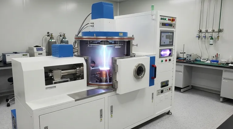
In essence, electron beam evaporation is a physical vapor deposition (PVD) technique that uses a focused, high-energy beam of electrons to heat a source material inside a vacuum chamber. This intense, targeted heating converts the material into a vapor, which then travels and condenses onto a cooler substrate, forming an exceptionally pure and uniform thin film.
The core principle is the conversion of kinetic energy into thermal energy. By precisely controlling a beam of electrons, the process can vaporize even materials with extremely high melting points, offering superior control and purity compared to other deposition methods.
Deconstructing the E-Beam Evaporation Process
To truly understand this technique, we must break it down into its fundamental stages. Each step is critical for achieving a high-quality thin film.
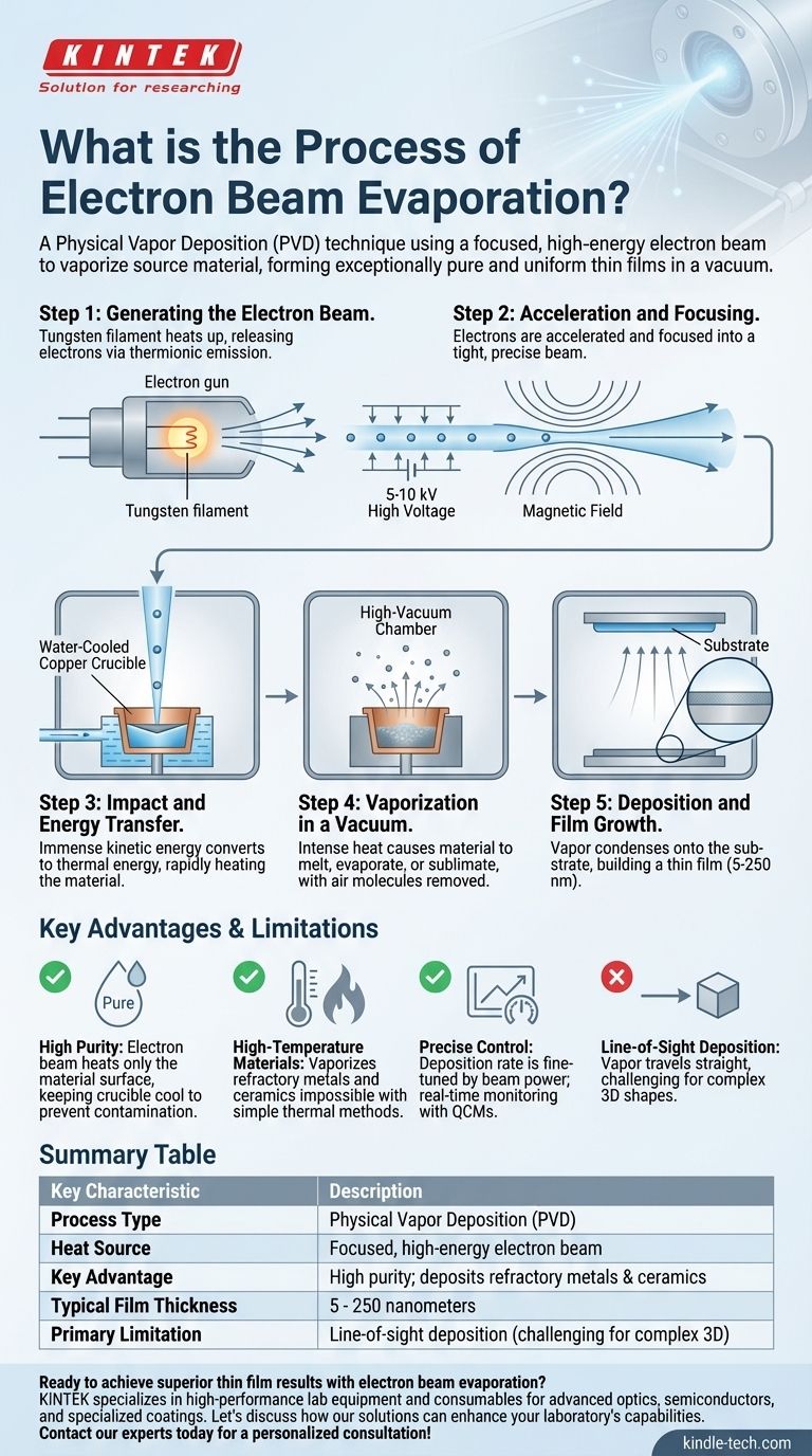
Step 1: Generating the Electron Beam
The process begins with an electron gun. A current is passed through a tungsten filament, heating it to a very high temperature.
This extreme heat causes the filament to release electrons through a process called thermionic emission.
Step 2: Acceleration and Focusing
Once freed, the electrons are accelerated by a high voltage, typically between five and ten kilovolts (kV), giving them significant kinetic energy.
A magnetic field is then used to focus these fast-moving electrons into a tight, precise beam, allowing for accurate targeting.
Step 3: Impact and Energy Transfer
This focused beam is directed toward the source material, which sits in a water-cooled copper crucible or hearth.
Upon impact, the immense kinetic energy of the electrons is instantly converted into thermal energy, causing a rapid and localized increase in the material's temperature.
Step 4: Vaporization in a Vacuum
The intense heat causes the source material to either melt and evaporate or, in some cases, sublimate directly from a solid to a gas.
This entire process occurs within a high-vacuum chamber. The vacuum is crucial because it removes air molecules that would otherwise interfere with or react with the vaporized material.
Step 5: Deposition and Film Growth
The vaporized material travels in a straight line from the source toward the substrate, which is strategically positioned above.
Upon reaching the cooler substrate surface, the vapor condenses back into a solid state, gradually building up a thin film. The thickness of this film typically ranges from 5 to 250 nanometers.
Understanding the Trade-offs and Key Advantages
No single technique is perfect for every application. Understanding the benefits and limitations of e-beam evaporation is essential for making an informed decision.
The Advantage: High Purity
Because the electron beam heats only the surface of the source material, the water-cooled crucible remains cool. This prevents the crucible material from melting and contaminating the vapor stream, resulting in films of very high purity.
The Advantage: High-Temperature Materials
The energy transfer is so efficient that e-beam evaporation can vaporize materials with extremely high melting points, such as refractory metals and ceramics, which are impossible to process with simpler thermal evaporation methods.
The Advantage: Precise Control
The deposition rate is directly related to the power of the electron beam. This allows for fine-tuning of the process, often in real-time using monitors like Quartz Crystal Microbalances (QCMs), to achieve highly precise film thicknesses.
The Limitation: Line-of-Sight Deposition
The vaporized material travels in a straight line from the source to the substrate. This "line-of-sight" characteristic means it is excellent for coating flat surfaces but can struggle to uniformly coat complex, three-dimensional shapes without sophisticated substrate manipulation.
The Consideration: System Complexity
E-beam evaporators are more complex and require a larger initial investment than simpler thermal deposition systems due to the need for a high-voltage power supply, electron gun, and magnetic focusing systems.
Making the Right Choice for Your Goal
Selecting the correct deposition method depends entirely on your specific requirements for material, purity, and precision.
- If your primary focus is exceptional material purity and depositing refractory metals or ceramics: E-beam evaporation is the superior choice due to its direct, non-contaminating heating method.
- If your primary focus is precise thickness control for advanced optics or electronics: The fine control over deposition rate makes e-beam evaporation an ideal solution for creating complex, multi-layered structures.
- If your primary focus is coating simple materials on a limited budget: A less complex method like standard thermal evaporation might be a more suitable and cost-effective alternative.
Ultimately, understanding the mechanics of electron beam evaporation empowers you to select the ideal manufacturing process for creating high-performance thin films.
Summary Table:
| Key Characteristic | Description |
|---|---|
| Process Type | Physical Vapor Deposition (PVD) |
| Heat Source | Focused, high-energy electron beam |
| Key Advantage | High purity; can deposit refractory metals & ceramics |
| Typical Film Thickness | 5 - 250 nanometers |
| Primary Limitation | Line-of-sight deposition (challenging for complex 3D shapes) |
Ready to achieve superior thin film results with electron beam evaporation?
KINTEK specializes in providing high-performance lab equipment and consumables for all your deposition needs. Whether you are developing advanced optics, semiconductors, or specialized coatings, our expertise ensures you get the purity and precision your research demands.
Let's discuss how our solutions can enhance your laboratory's capabilities. Contact our experts today for a personalized consultation!
Visual Guide
Related Products
- Electron Beam Evaporation Coating Oxygen-Free Copper Crucible and Evaporation Boat
- Electron Beam Evaporation Coating Tungsten Crucible and Molybdenum Crucible for High Temperature Applications
- Electron Beam Evaporation Coating Gold Plating Tungsten Molybdenum Crucible for Evaporation
- Electron Beam Evaporation Coating Conductive Boron Nitride Crucible BN Crucible
- E Beam Crucibles Electron Gun Beam Crucible for Evaporation
People Also Ask
- What are the applications of e-beam evaporation? Achieve High-Purity Coatings for Optics & Electronics
- What is the temperature of e-beam evaporation? Mastering the Two-Zone Thermal Process for Precision Films
- What is e-beam evaporation used for? Precision Coating for Optics, Aerospace & Electronics
- What is the current of e-beam evaporation? A Guide to High-Purity Thin Film Deposition
- What is e-beam evaporation? Achieve High-Purity Thin Film Deposition for Your Lab


