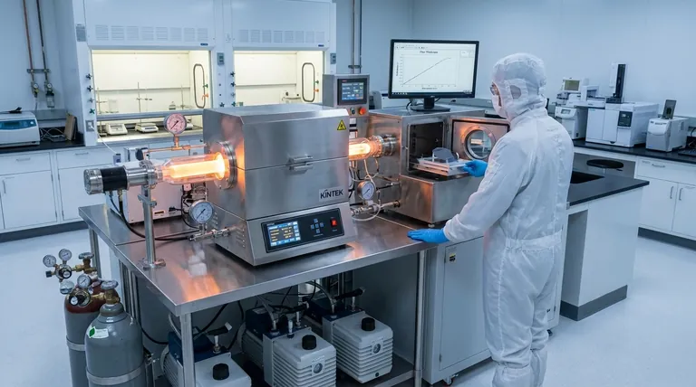
At its core, film deposition is a process where a material is converted into a vapor, transported, and then condensed onto a surface, known as a substrate, to form an extremely thin layer. This entire sequence is conducted in a highly controlled environment, typically a vacuum, to ensure the purity and desired properties of the resulting film.
The success of any film deposition process does not lie in a single step, but in the meticulous execution of a multi-stage sequence. From preparing the substrate to controlling the deposition environment and choosing the right material transport mechanism, each phase is critical for achieving the final film's required thickness, purity, and structure.
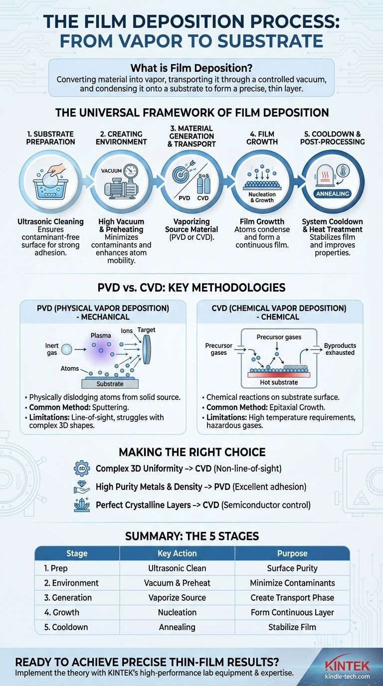
The Universal Framework of Film Deposition
Almost all thin-film deposition techniques, whether physical or chemical, follow a similar five-stage chronological framework. Understanding this sequence is essential for diagnosing issues and optimizing results.
Stage 1: Substrate Preparation
Before deposition can begin, the substrate surface must be immaculately clean. Any contaminants will compromise the film's adhesion and purity.
This stage typically involves ultrasonic cleaning in various solvents to remove oils and particulates. The cleaned substrate is then securely fastened to a holder inside the deposition chamber.
Stage 2: Creating the Deposition Environment
The process requires a highly controlled environment, which usually means creating a vacuum.
The chamber is evacuated to a high vacuum to minimize background gases and contaminants. This "ramp up" phase ensures that only the intended materials are part of the process. The substrate may also be preheated to enhance the mobility of deposited atoms, leading to a denser and more uniform film.
Stage 3: Generation and Transport of Material
This is the point where the source material, or "target," is converted into a vapor phase so it can travel to the substrate.
The method of generation is the primary distinction between different deposition families. The material might be physically ejected by ion bombardment (PVD) or synthesized from precursor gases (CVD).
Stage 4: Film Growth on the Substrate
As the vaporized material arrives at the substrate, it condenses and begins to form a film.
This involves atoms adsorbing onto the surface, diffusing to find stable growth sites, and eventually forming a continuous layer through a process called nucleation and growth.
Stage 5: System Cooldown and Post-Processing
Once the desired film thickness is achieved, the process is stopped, and the system begins its "ramp down" phase.
The chamber is carefully returned to ambient temperature and pressure. In some cases, the film may undergo annealing—a form of heat treatment—to improve its crystalline structure or other properties.
Key Deposition Methodologies: PVD vs. CVD
While the five-stage framework is universal, the specifics of Stage 3 (generation and transport) define the two primary categories of deposition: Physical Vapor Deposition (PVD) and Chemical Vapor Deposition (CVD).
Physical Vapor Deposition (PVD): A Mechanical Approach
PVD involves physically dislodging atoms from a solid source material and having them deposit on the substrate.
In sputtering, a common PVD method, a chamber is filled with an inert gas like argon. This gas is energized into a plasma, and its ions are accelerated to strike the source target, physically knocking atoms off, which then travel and coat the substrate.
Chemical Vapor Deposition (CVD): A Chemical Approach
CVD builds a film through chemical reactions that occur directly on the substrate's surface.
Volatile precursor gases are introduced into the chamber. At the hot substrate surface, these gases decompose or react with each other. The nonvolatile products of this reaction deposit onto the surface, building the film atom by atom, while gaseous byproducts are exhausted.
Understanding the Trade-offs
Neither PVD nor CVD is universally superior; the choice depends entirely on the application and desired film characteristics.
PVD Limitations
PVD is typically a line-of-sight process. This means it is excellent for coating flat surfaces but struggles to uniformly coat complex, three-dimensional shapes with undercuts or hidden areas.
CVD Limitations
The chemical nature of CVD often requires very high substrate temperatures to drive the necessary reactions. Furthermore, the precursor gases can be highly toxic, flammable, or corrosive, demanding significant safety infrastructure.
The Critical Role of Control
Both methods require extremely precise control over process parameters. Factors like pressure, temperature, gas flow, and power levels must be tightly regulated, as even minor deviations can dramatically alter the final film's properties.
Making the Right Choice for Your Goal
Your application's specific requirements will dictate the most appropriate deposition method.
- If your primary focus is coating a complex 3D part uniformly: CVD is generally the superior choice due to its non-line-of-sight nature, allowing precursor gases to reach all surfaces.
- If your primary focus is depositing a pure metal or alloy with high density: PVD methods like sputtering are industry-standard, known for producing high-purity films with excellent adhesion.
- If your primary focus is growing highly perfect, crystalline layers for electronics: CVD is the dominant technology in the semiconductor industry for its ability to create epitaxial films with exceptional control.
Ultimately, mastering film deposition comes from understanding this fundamental framework and then selecting the specific method whose trade-offs best align with your final objective.
Summary Table:
| Stage | Key Action | Purpose |
|---|---|---|
| 1. Substrate Preparation | Ultrasonic Cleaning & Mounting | Ensures a contaminant-free surface for strong film adhesion. |
| 2. Environment Creation | Vacuum Pumping & Preheating | Minimizes contaminants and prepares the substrate for deposition. |
| 3. Material Generation | Vaporizing the Source (PVD/CVD) | Creates the vapor phase of the material for transport. |
| 4. Film Growth | Nucleation & Condensation | Atoms form a continuous, uniform layer on the substrate. |
| 5. Cooldown & Processing | Annealing & Pressure Return | Stabilizes the film and improves its final properties. |
Ready to Achieve Precise Thin-Film Results?
Understanding the theory is the first step; implementing it requires the right equipment and expertise. KINTEK specializes in high-performance lab equipment and consumables for all your deposition needs, whether you're working with PVD, CVD, or other advanced techniques.
We provide the reliable tools and expert support to help your laboratory:
- Ensure Process Control: Achieve the precise parameters needed for consistent, high-quality films.
- Select the Right Method: Get guidance on whether PVD or CVD is best for your specific material and application.
- Optimize Your Workflow: From substrate preparation to final annealing, streamline your entire deposition process.
Let's discuss your project requirements. Contact our experts today to find the perfect solution for your laboratory's thin-film challenges.
Visual Guide
Related Products
- Aluminized Ceramic Evaporation Boat for Thin Film Deposition
- Tungsten Evaporation Boat for Thin Film Deposition
- Electron Beam Evaporation Coating Oxygen-Free Copper Crucible and Evaporation Boat
- Molybdenum Tungsten Tantalum Evaporation Boat for High Temperature Applications
- HFCVD Machine System Equipment for Drawing Die Nano-Diamond Coating
People Also Ask
- What is the chemical method for thin film deposition? Build Films from the Molecular Level Up
- Why is an alumina boat and Ti3AlC2 powder bed necessary for Ti2AlC sintering? Protect MAX Phase Purity
- What are thin films deposited by evaporation? A Guide to High-Purity Coating
- What is the source of evaporation for thin film? Choosing Between Thermal and E-Beam Methods
- What are the alternatives to sputtering? Choose the Right Thin Film Deposition Method


