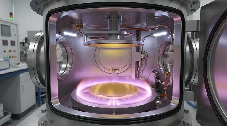
Gold sputtering is a high-precision coating technique used to deposit an exceptionally thin and uniform layer of gold onto a surface. In a high-vacuum chamber, a solid gold "target" is bombarded with energetic ions from an inert gas, like argon. This bombardment physically knocks individual gold atoms off the target, which then travel and land on a nearby object, known as a substrate, forming a consistent and high-quality film.
At its core, gold sputtering is not about simply covering a surface; it's a method for engineering a film with unparalleled control. It enables the creation of ultra-thin, highly uniform gold layers with specific electrical and optical properties that are often impossible to achieve with other methods like electroplating or simple evaporation.
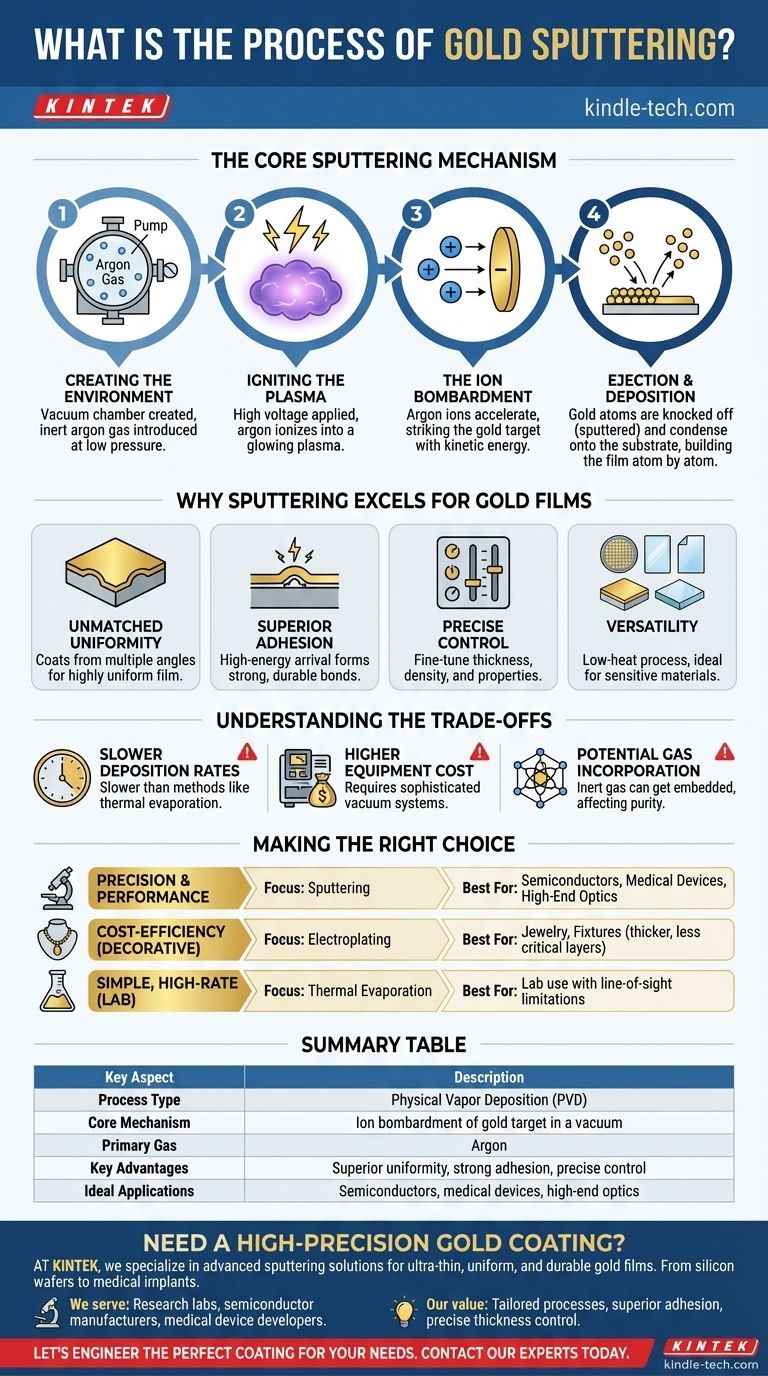
The Core Sputtering Mechanism
To understand why sputtering is so effective, it's essential to break down the process into its key physical stages. The entire operation takes place inside a sealed vacuum chamber to ensure purity and control.
Step 1: Creating the Environment
The substrate (the object to be coated) and the gold target are placed in a vacuum chamber. All air is pumped out, creating a near-vacuum. A small amount of a chemically inert gas, most commonly argon, is then introduced at very low pressure.
Step 2: Igniting the Plasma
A high voltage is applied between the target and the substrate, with the gold target acting as the negative electrode (cathode). This strong electric field energizes the chamber, stripping electrons from the argon atoms and creating a glowing, ionized gas known as a plasma.
Step 3: The Ion Bombardment
The positively charged argon ions within the plasma are now forcefully accelerated toward the negatively charged gold target. They strike the target's surface with significant kinetic energy.
Step 4: Ejection and Deposition
This bombardment acts like a microscopic billiard game, transferring momentum from the argon ions to the gold atoms. This process, known as a collision cascade, gives some surface atoms enough energy to break their metallic bonds and be ejected from the target. These free gold atoms travel in a vapor stream through the low-pressure chamber and condense onto the substrate, gradually building the thin film atom by atom.
Why Sputtering Excels for Gold Films
While other methods can deposit gold, sputtering is chosen when the quality and properties of the final film are critical.
Unmatched Film Uniformity
Because sputtered atoms are ejected from the target in various directions, they coat the substrate from multiple angles. This leads to a highly uniform film that can cover microscopic surface textures more effectively than line-of-sight methods like thermal evaporation.
Superior Adhesion
The sputtered gold atoms arrive at the substrate with considerable energy. This energy helps them form a stronger physical and chemical bond with the substrate surface, resulting in a durable film that is less likely to flake or peel.
Precise Control Over Film Properties
Technicians can precisely control the film's thickness, density, and even grain structure by fine-tuning the gas pressure, voltage, and deposition time. This allows for the engineering of films with specific electrical resistivity for electronics or reflectivity for optics.
Versatility of Substrates
Sputtering is a relatively low-heat process compared to some alternatives. This makes it ideal for coating heat-sensitive materials, such as plastics, glass, and advanced semiconductor components like silicon wafers.
Understanding the Trade-offs
No technique is perfect. To make an informed decision, you must be aware of the limitations of gold sputtering.
Slower Deposition Rates
Sputtering is fundamentally a physical process of knocking atoms loose one by one. It is generally slower than thermal evaporation, where material is boiled off, making it less suitable for applications requiring very thick coatings or extremely high throughput.
Higher Equipment Complexity and Cost
Sputtering systems require sophisticated vacuum chambers, high-voltage power supplies, and precise gas flow controllers. This initial investment in equipment is significantly higher than for simpler methods like electroplating.
Potential for Gas Incorporation
In some cases, the inert gas ions (e.g., argon) used for bombardment can become embedded in the growing gold film. This can slightly alter the film's purity and its electrical or mechanical properties, which must be managed for highly sensitive applications.
Making the Right Choice for Your Application
Selecting the right coating method depends entirely on your project's primary goal.
- If your primary focus is ultimate precision and performance: Choose sputtering for its superior film uniformity, strong adhesion, and fine-grained control, which is critical for semiconductors, medical devices, and high-end optics.
- If your primary focus is cost-efficiency for decorative purposes: Consider electroplating, which is faster and cheaper for applying thicker, less structurally critical gold layers on jewelry or fixtures.
- If your primary focus is simple, high-rate deposition in a lab: Thermal evaporation can be a viable, lower-cost alternative to sputtering, provided you can tolerate its line-of-sight limitations and weaker film adhesion.
Ultimately, choosing gold sputtering is a decision to prioritize the quality, precision, and performance of the final film over process speed or initial cost.
Summary Table:
| Key Aspect | Description |
|---|---|
| Process Type | Physical Vapor Deposition (PVD) |
| Core Mechanism | Ion bombardment of gold target in a vacuum |
| Primary Gas Used | Argon |
| Key Advantages | Superior uniformity, strong adhesion, precise control |
| Ideal Applications | Semiconductors, medical devices, high-end optics |
| Main Limitations | Slower deposition rate, higher equipment cost |
Need a high-precision gold coating for your critical application?
At KINTEK, we specialize in advanced sputtering solutions for laboratories and industries requiring ultra-thin, uniform, and durable gold films. Our expertise ensures your substrates—from silicon wafers to medical implants—receive the exact properties needed for optimal performance.
🔬 We serve: Research labs, semiconductor manufacturers, medical device developers, and optics engineers.
💡 Our value: Tailored sputtering processes that deliver superior adhesion, precise thickness control, and consistent results for your most demanding projects.
Let's engineer the perfect coating for your needs. Contact our experts today to discuss your specific requirements!
Visual Guide
Related Products
- Electron Beam Evaporation Coating Gold Plating Tungsten Molybdenum Crucible for Evaporation
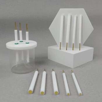
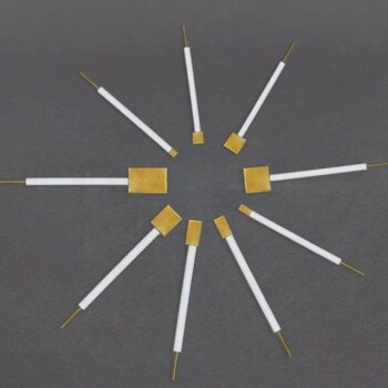
- Gold Disc Electrode
- Gold Electrochemical Sheet Electrode Gold Electrode
People Also Ask
- What is the temperature of e-beam evaporation? Mastering the Two-Zone Thermal Process for Precision Films
- What is the container that holds the metal source material called in e-beam evaporation? Ensure Purity and Quality in Your Thin-Film Deposition
- What materials are used in electron beam evaporation? Master High-Purity Thin Film Deposition
- What is the voltage of e-beam evaporation? Achieve Precise Thin-Film Deposition
- What is the process of e-beam coating? Achieve High-Purity, Precise Thin Films for Your Lab