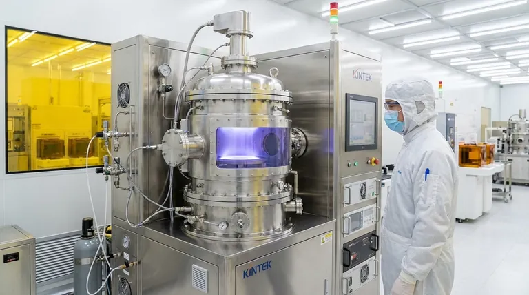
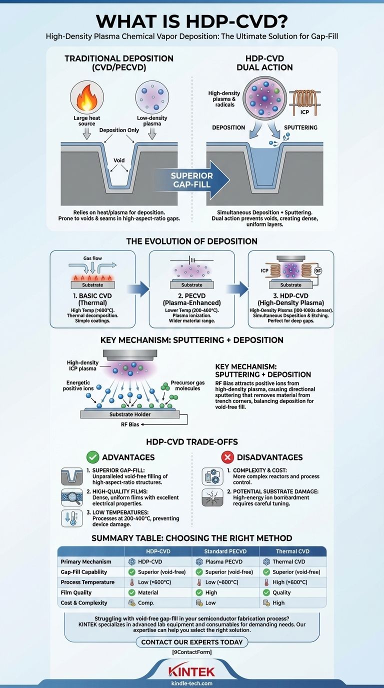
In short, High-Density Plasma Chemical Vapor Deposition (HDP-CVD) is an advanced process used to deposit high-quality thin films, especially for filling microscopic, high-aspect-ratio gaps in semiconductor manufacturing. Unlike standard Chemical Vapor Deposition (CVD), which relies primarily on heat, HDP-CVD uses an inductively coupled, high-density plasma to both deposit material and simultaneously sputter it away. This dual action prevents voids from forming and creates a dense, uniform layer.
The critical difference in HDP-CVD is its ability to perform simultaneous deposition and etching. This unique characteristic allows it to fill deep, narrow trenches without creating the voids or seams that plague less advanced deposition methods.
The Foundation: Understanding Basic CVD
What is Chemical Vapor Deposition?
Chemical Vapor Deposition (CVD) is a foundational process for producing high-performance, solid materials as thin films. It involves introducing one or more volatile precursor gases into a reaction chamber.
These gases react or decompose on a heated substrate surface, resulting in the deposition of the desired solid material. The resulting film can be crystalline or amorphous.
The Role of Energy
In traditional thermal CVD, high temperatures (often >600°C) provide the necessary energy to break chemical bonds in the precursor gases and drive the deposition reaction.
The properties of the final film are controlled by adjusting conditions like temperature, pressure, and the specific gases used.
The Evolution to High-Density Plasma
Moving Beyond Heat: Plasma-Enhanced CVD (PECVD)
To deposit films at lower temperatures, Plasma-Enhanced CVD (PECVD) was developed. Instead of relying solely on thermal energy, PECVD uses an electric field to ionize the precursor gases, creating a plasma.
This plasma contains highly reactive ions and radicals that can deposit a film at much lower temperatures (typically 200-400°C), making it suitable for a wider range of materials.
Why "High-Density" Plasma Matters
HDP-CVD is a specialized form of PECVD. It utilizes a plasma that is significantly more ionized—typically 100 to 1,000 times denser—than that used in conventional PECVD systems.
This high-density plasma is usually generated by an inductively coupled plasma (ICP) source, which efficiently transfers energy into the gas. This allows the process to run at lower pressures, improving film purity and uniformity.
The Core Mechanism: Sputtering + Deposition
The defining feature of HDP-CVD is the application of a separate radio-frequency (RF) bias to the substrate holder (the wafer chuck).
This bias attracts positive ions from the high-density plasma, causing them to accelerate toward the substrate. These energetic ions physically bombard the surface, a process known as sputtering.
The result is a dynamic equilibrium: precursor gases are constantly depositing a film, while the sputtering action is constantly etching it away. Because the sputtering is highly directional (perpendicular to the surface), it preferentially removes material from the top corners of a trench, keeping it open and allowing the bottom to fill completely.
Understanding the Trade-offs
Advantage: Superior Gap-Fill
The primary reason for using HDP-CVD is its unparalleled ability to achieve void-free filling of high-aspect-ratio structures, such as the gaps between metal lines on an integrated circuit. No other deposition technique performs this task as effectively.
Advantage: High-Quality Films at Low Temperatures
The high-density plasma produces a dense, high-quality film with excellent electrical and mechanical properties. This is achieved at a relatively low substrate temperature, preventing damage to underlying device structures.
Disadvantage: Process Complexity and Cost
HDP-CVD reactors are significantly more complex and expensive than standard PECVD or thermal CVD systems. The need for separate plasma generation and substrate biasing sources adds to the cost and process control challenges.
Disadvantage: Potential for Substrate Damage
The high-energy ion bombardment that enables the sputtering effect can also cause physical damage to the substrate surface. This requires careful tuning of the process parameters to balance the benefits of gap-fill against the risk of device damage.
Making the Right Choice for Your Application
The choice of deposition method depends entirely on the geometric and thermal constraints of your application.
- If your primary focus is void-free filling of deep, narrow trenches: HDP-CVD is the definitive and often only viable solution.
- If your primary focus is a simple conformal coating on a relatively flat surface: Standard PECVD is a more cost-effective and simpler alternative.
- If your primary focus is achieving the highest purity on a temperature-tolerant substrate: Traditional high-temperature thermal CVD might still be the best choice.
Ultimately, HDP-CVD is a specialized tool engineered to solve one of the most difficult challenges in modern microfabrication: perfectly filling gaps that are much deeper than they are wide.
Summary Table:
| Feature | HDP-CVD | Standard PECVD | Thermal CVD |
|---|---|---|---|
| Primary Mechanism | Simultaneous deposition & sputtering | Plasma-enhanced deposition | Thermal decomposition |
| Gap-Fill Capability | Superior (void-free) | Limited | Poor |
| Process Temperature | Low (200-400°C) | Low (200-400°C) | High (>600°C) |
| Film Quality | Dense, high-quality | Good | High purity |
| Cost & Complexity | High | Moderate | Low to Moderate |
Struggling with void-free gap-fill in your semiconductor fabrication process? KINTEK specializes in advanced lab equipment and consumables for demanding laboratory needs. Our expertise in deposition technologies can help you select the right solution for your specific application.
Contact our experts today via our Contact Form to discuss how our solutions can enhance your microfabrication process and achieve superior results.
Visual Guide
Related Products
- HFCVD Machine System Equipment for Drawing Die Nano-Diamond Coating
- Chemical Vapor Deposition CVD Equipment System Chamber Slide PECVD Tube Furnace with Liquid Gasifier PECVD Machine
- Microwave Plasma Chemical Vapor Deposition MPCVD Machine System Reactor for Lab and Diamond Growth
- 915MHz MPCVD Diamond Machine Microwave Plasma Chemical Vapor Deposition System Reactor
- Cylindrical Resonator MPCVD Machine System Reactor for Microwave Plasma Chemical Vapor Deposition and Lab Diamond Growth
People Also Ask
- How expensive is chemical vapor deposition? Understanding the True Cost of High-Performance Coating
- Why is Chemical Vapor Deposition (CVD) equipment uniquely suited for constructing hierarchical superhydrophobic structures?
- What are the advantages of chemical vapor deposition? Achieve Superior Thin Films for Your Lab
- What is the full form of HFCVD? A Guide to Hot Filament Chemical Vapor Deposition
- What is the chemical vapor deposition growth process? Build Superior Thin Films from the Atom Up


