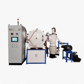
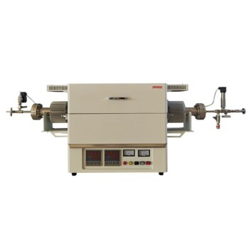
In essence, Physical Vapor Deposition (PVD) is a vacuum-based process that transfers a coating material from a solid source to a part's surface on an atom-by-atom basis. The process involves three fundamental steps: a solid target material is converted into a vapor, this vapor travels through a vacuum chamber, and it then condenses onto the substrate to form a thin, highly durable film. Critically, this is a purely physical process, involving no chemical reactions.
The core principle of PVD is straightforward: it transforms a solid into a vapor and then back into a solid on a different surface. Think of it as being similar to how water vapor (gas) from a boiling kettle condenses into a film of water (liquid) on a cool window pane, but done under a vacuum with high-energy materials to create a solid, atom-thin coating.

The Core Principles of PVD
To understand the PVD process, it's essential to grasp the environment and the physical principles that make it work. The entire process is engineered to ensure a pure, dense, and well-adhered coating.
The Vacuum Environment is Critical
The entire PVD process takes place in a chamber under a very high vacuum (very low pressure).
This vacuum is essential for two reasons. First, it removes air and other gas molecules that could react with or contaminate the coating material. Second, it provides a clear, unobstructed path for the vaporized atoms to travel from their source to the part being coated.
The Solid-to-Vapor Transition
The goal of the first stage is to liberate atoms from a solid source material, known as the target. This target is made of the pure material you wish to deposit as a coating, such as titanium, chromium, or gold.
By applying high energy, the bonds holding the solid target together are broken, and individual atoms or molecules are ejected into the vacuum chamber, forming a cloud of vapor.
Atom-by-Atom Deposition
Once vaporized, the atoms travel in a straight line through the vacuum and strike the surface of the part, or substrate.
Upon impact, they condense back into a solid state, building up a thin film layer by layer, atom by atom. This method creates an exceptionally dense, pure, and uniform coating.
The Three Fundamental Stages of the PVD Process
While there are different PVD techniques, they all follow the same three-stage sequence. The primary difference between methods lies in how the first stage—vaporization—is accomplished.
Stage 1: Vaporization
This is the most energy-intensive step, where the solid coating material is converted into a gaseous vapor. The method used defines the type of PVD process.
Common methods include thermal evaporation, where the target is heated until it boils and evaporates, or sputtering, where the target is bombarded with high-energy ions (a plasma) that physically knock atoms off its surface.
Stage 2: Transportation
This is the simplest stage. The vaporized atoms travel from the target to the substrate through the vacuum chamber.
Because of the vacuum, the atoms face minimal interference and travel in a direct "line of sight" path to the parts being coated.
Stage 3: Deposition
In the final stage, the vaporized material condenses on the surface of the substrate.
The properties of the final coating—such as its hardness, density, and adhesion—are carefully controlled by managing variables like temperature, pressure, and the energy of the depositing atoms.
Understanding the Trade-offs
PVD is a powerful technology, but it's important to understand its specific characteristics and limitations to determine if it's the right choice for an application.
Strength: High Purity and Hardness
Because the process occurs in a vacuum with pure source materials, PVD coatings are extremely pure and free from contamination. This results in very hard, dense, and wear-resistant finishes.
Strength: Low-Temperature Application
Compared to other coating processes like Chemical Vapor Deposition (CVD), PVD can be performed at relatively low temperatures. This makes it suitable for coating heat-sensitive materials, such as plastics or certain metal alloys, without damaging them.
Limitation: Line-of-Sight Process
The atoms travel in a straight line from the target to the substrate. This means PVD is excellent for coating external surfaces but struggles to uniformly coat the inside of complex geometries or hidden areas that are not in the direct line of sight of the vapor source.
How to Apply This to Your Goal
Choosing a coating process depends entirely on the desired outcome. PVD excels in applications where performance, precision, and appearance are paramount.
- If your primary focus is durability and wear resistance: PVD is a leading choice for creating hard, lubricious coatings on cutting tools, engine components, and industrial equipment.
- If your primary focus is a high-quality aesthetic finish: PVD provides brilliant, durable, and tarnish-resistant decorative coatings for items like watches, faucets, and consumer electronics.
- If your primary focus is a high-performance thin film: PVD is essential in the manufacturing of semiconductors, optical lenses, and solar panels where ultra-thin, highly pure layers are required.
Ultimately, the PVD process is a highly controlled physical technique for creating superior thin-film coatings by moving material at an atomic level.
Summary Table:
| Stage | Key Action | Purpose |
|---|---|---|
| 1. Vaporization | Solid target material is converted into a vapor. | Liberate atoms from the source material. |
| 2. Transportation | Vaporized atoms travel through a vacuum chamber. | Ensure a pure, direct path to the substrate. |
| 3. Deposition | Atoms condense onto the substrate surface. | Build a dense, uniform, atom-thin coating layer by layer. |
Ready to enhance your products with high-performance PVD coatings? KINTEK specializes in advanced lab equipment and consumables for precise thin-film deposition. Whether you're developing cutting tools, optical components, or durable decorative finishes, our solutions deliver the purity, hardness, and reliability your laboratory demands. Contact our experts today to discuss how we can support your specific coating challenges and goals.
Visual Guide

Related Products
- RF PECVD System Radio Frequency Plasma-Enhanced Chemical Vapor Deposition RF PECVD
- Split Chamber CVD Tube Furnace with Vacuum Station Chemical Vapor Deposition System Equipment Machine
- Chemical Vapor Deposition CVD Equipment System Chamber Slide PECVD Tube Furnace with Liquid Gasifier PECVD Machine
- VHP Sterilization Equipment Hydrogen Peroxide H2O2 Space Sterilizer
- Aluminized Ceramic Evaporation Boat for Thin Film Deposition
People Also Ask
- What are the applications of PECVD? Essential for Semiconductors, MEMS, and Solar Cells
- Why is PECVD environment friendly? Understanding the Eco-Friendly Benefits of Plasma-Enhanced Coating
- How are PECVD and CVD different? A Guide to Choosing the Right Thin-Film Deposition Process
- How does RF power create plasma? Achieve Stable, High-Density Plasma for Your Applications
- What is an example of PECVD? RF-PECVD for High-Quality Thin Film Deposition

