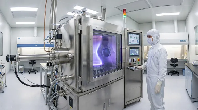
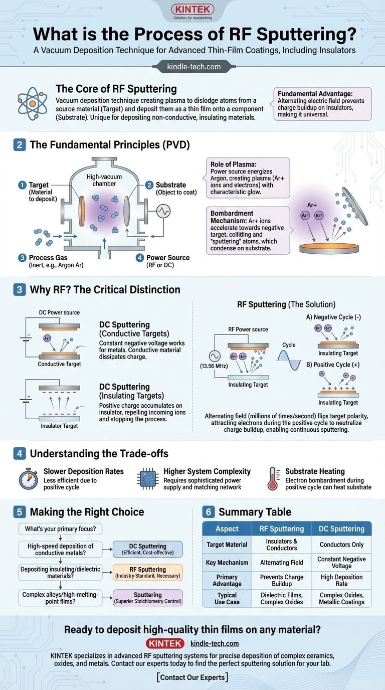
At its core, RF sputtering is a vacuum deposition technique that uses a radio-frequency (RF) power source to create a plasma. This plasma bombards a source material (the "target"), dislodging atoms that then travel and deposit as a thin, uniform film onto a component (the "substrate"). Its unique ability to deposit non-conductive, insulating materials makes it one of the most versatile methods for creating high-performance coatings.
The fundamental advantage of RF sputtering is its alternating electric field. This rapid switching prevents the electrical charge buildup that otherwise stops the process when working with insulating materials, making it a universal tool for depositing virtually any type of film.
The Fundamental Principles of Sputtering
Before focusing on RF, it's crucial to understand the basic mechanism of sputtering, which is a form of Physical Vapor Deposition (PVD). The entire process occurs inside a high-vacuum chamber.
The Key Components
The system has four essential elements:
- The Target: A solid plate of the material you want to deposit.
- The Substrate: The object you want to coat (e.g., a silicon wafer, glass, or a medical implant).
- The Process Gas: An inert gas, most commonly Argon (Ar), that is introduced into the vacuum chamber.
- The Power Source: An electrical supply that provides the energy to drive the process.
The Role of Plasma
Once the chamber is pumped to a high vacuum, a small amount of Argon gas is introduced. The power source is then activated, applying a strong electric field that energizes the chamber.
This energy strips electrons from the Argon atoms, creating a mixture of positively charged Argon ions (Ar+) and free electrons. This ionized gas is known as a plasma, often visible as a characteristic glow.
The Bombardment Mechanism
The target material is given a strong negative electrical potential, making it the cathode. The positive Argon ions in the plasma are naturally accelerated by the electric field and collide with the negatively charged target at high speed.
Each collision transfers kinetic energy from the ion to the target material, which can be enough to knock out, or "sputter," individual atoms from the target's surface. These ejected atoms travel through the low-pressure chamber and condense on the substrate, gradually building up a thin film.
Why "RF"? The Critical Distinction
The choice between a direct current (DC) and a radio frequency (RF) power source is the most important decision in sputtering, as it dictates what materials you can deposit.
The Problem with DC Sputtering
In a standard DC system, a constant negative voltage is applied to the target. This works perfectly for conductive targets like metals because the material can easily dissipate the positive charge delivered by the bombarding ions.
Charge Buildup on Insulators
If you try to use a DC source with an insulating target (like a ceramic or oxide), the process quickly fails. As positive Argon ions strike the surface, their charge accumulates.
The insulating material cannot conduct this charge away. Very quickly, the target surface develops a strong positive charge that repels any more incoming positive Argon ions, effectively shutting down the sputtering process.
The RF Solution: The Alternating Field
RF sputtering solves this problem by using an alternating power source, typically at a standard industrial frequency of 13.56 MHz. The electric field rapidly flips between negative and positive millions of times per second.
- During the negative half-cycle: The target is negatively charged, attracting Argon ions for bombardment and sputtering atoms just like in a DC system.
- During the positive half-cycle: The target briefly becomes positive. It now attracts the highly mobile, negatively charged electrons from the plasma. This flood of electrons completely neutralizes the positive charge that built up during the previous cycle.
This "self-cleaning" action ensures the target surface is always ready for the next bombardment cycle, allowing for the continuous and stable sputtering of any insulating material.
Understanding the Trade-offs
While incredibly versatile, RF sputtering is not always the optimal choice. Understanding its limitations is key to making an informed decision.
Slower Deposition Rates
The sputtering process primarily occurs during the negative portion of the RF cycle. Because the cycle also includes a positive, "non-sputtering" phase, the overall deposition rate of RF sputtering is generally lower than that of DC sputtering for the same material.
Higher System Complexity
An RF power system requires a sophisticated power supply and an impedance-matching network to efficiently deliver power to the plasma. This makes RF systems more complex and expensive than their DC counterparts.
Substrate Heating
During the positive cycle, the target surface is bombarded by electrons. This can lead to additional heating of the target and, through radiation, the substrate. For heat-sensitive substrates, this effect must be carefully managed.
Making the Right Choice for Your Goal
Selecting the correct sputtering technique depends entirely on the material you need to deposit and your performance requirements.
- If your primary focus is high-speed deposition of conductive metals: DC sputtering is almost always the more efficient and cost-effective choice.
- If your primary focus is depositing insulating or dielectric materials (e.g., SiO₂, Al₂O₃): RF sputtering is the industry-standard and necessary method.
- If your primary focus is creating films from complex alloys or high-melting-point materials: Sputtering in general (both RF and DC) provides superior control over film stoichiometry compared to other methods like thermal evaporation.
By understanding how the alternating field overcomes the challenge of charge buildup, you can confidently select the right tool for your thin-film application.
Summary Table:
| Aspect | RF Sputtering | DC Sputtering |
|---|---|---|
| Target Material | Insulators (e.g., SiO₂, Al₂O₃) & Conductors | Conductors Only |
| Key Mechanism | Alternating Field (13.56 MHz) | Constant Negative Voltage |
| Primary Advantage | Prevents Charge Buildup on Insulators | High Deposition Rate for Metals |
| Typical Use Case | Dielectric Films, Complex Oxides | Metallic Coatings |
Ready to deposit high-quality thin films on any material?
KINTEK specializes in advanced lab equipment, including RF sputtering systems designed for precise deposition of both conductive and insulating materials. Whether you're working with complex ceramics, oxides, or metals, our solutions provide the control and reliability your research demands.
Let's discuss your specific coating challenges and find the perfect sputtering solution for your lab. Contact our experts today to learn how KINTEK can enhance your thin-film capabilities.
Visual Guide
Related Products
- RF PECVD System Radio Frequency Plasma-Enhanced Chemical Vapor Deposition RF PECVD
- Spark Plasma Sintering Furnace SPS Furnace
- Horizontal High Temperature Graphite Vacuum Graphitization Furnace
People Also Ask
- What is plasma enhanced chemical vapour deposition PECVD used for? Enable Low-Temp Thin Films for Electronics & Solar
- What is an example of PECVD? RF-PECVD for High-Quality Thin Film Deposition
- What is plasma chemical vapor deposition? A Low-Temperature Thin Film Coating Solution
- What is the role of RF-PECVD in VFG preparation? Mastering Vertical Growth and Surface Functionality
- How does plasma enhance CVD? Unlock Low-Temperature, High-Quality Film Deposition


