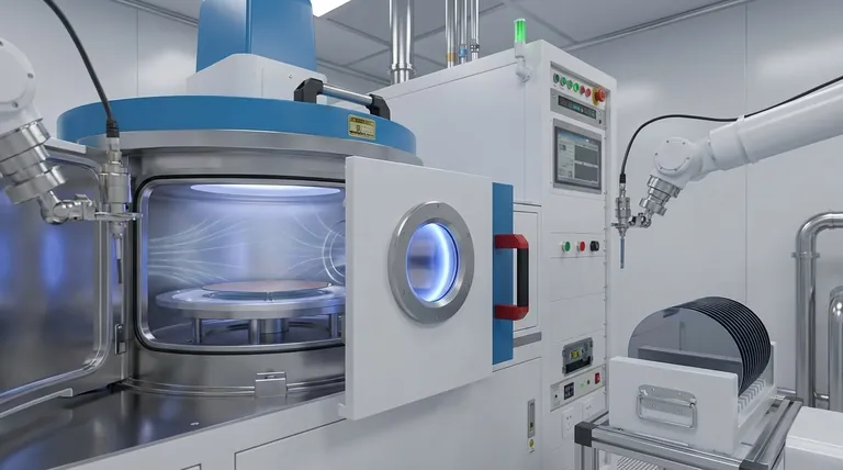
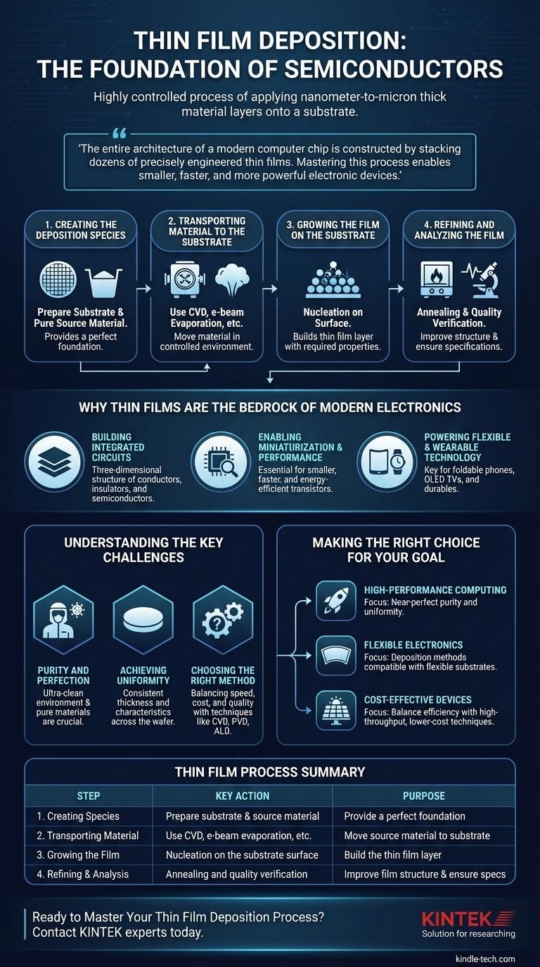
In semiconductor manufacturing, thin film deposition is the highly controlled process of applying a material layer, often just nanometers to microns thick, onto a base wafer called a substrate. This involves generating atoms or molecules from a source material, transporting them through a medium like a high vacuum, and carefully growing them on the substrate’s surface to build the foundational components of an integrated circuit.
The entire architecture of a modern computer chip is constructed by stacking dozens of precisely engineered thin films. Mastering this process is what enables the creation of smaller, faster, and more powerful electronic devices, from the processor in your phone to advanced LED displays.
The Core Steps of Thin Film Deposition
The creation of a thin film is a meticulous, multi-stage process where each step is critical to the final quality of the semiconductor device. The process can be broken down into a logical sequence, from preparing the base to verifying the final layer.
1. Creating the Deposition Species
The process begins with two key components: the substrate and the source material. The substrate is the base wafer, typically made of silicon, which has been cleaned and prepared to provide a perfect foundation. The source material, or target, is a highly pure substance that will form the film itself.
2. Transporting Material to the Substrate
Once the source material is ready, it must be transported to the substrate. This is the heart of the deposition process and is accomplished using various techniques, such as Chemical Vapor Deposition (CVD) or Electron Beam (e-beam) Evaporation, which occur in a controlled fluid or vacuum environment.
3. Growing the Film on the Substrate
As the source material arrives at the substrate's surface, it begins to form a layer. This growth phase, known as nucleation, is where individual atoms bond to the substrate and to each other, gradually building up the thin film with the required thickness and structural properties.
4. Refining and Analyzing the Film
After the initial deposition, the film may undergo annealing, a form of heat treatment, to improve its crystalline structure and electrical properties. Finally, the film is analyzed to ensure it meets specifications. This analysis provides a crucial feedback loop to modify and perfect the deposition process for future wafers.
Why Thin Films Are the Bedrock of Modern Electronics
Thin films are not merely a coating; they are the functional layers that give a semiconductor device its purpose. Their quality and precision directly dictate the performance and capabilities of the final product.
Building Integrated Circuits Layer by Layer
An integrated circuit, or computer chip, is essentially a three-dimensional structure built from a stack of different thin films. These layers consist of conductors (like copper), insulators (like silicon dioxide), and semiconductors (like doped silicon), which together form the billions of transistors that power a device.
Enabling Miniaturization and Performance
As electronic devices shrink, the role of thin films becomes even more critical. In a modern processor, these layers are incredibly thin, and even minor imperfections or variations in thickness can cause a device to fail. High-quality films are essential for creating smaller, faster, and more energy-efficient transistors.
Powering Flexible and Wearable Technology
Thin-film technology is the key enabler for next-generation devices like foldable smartphones, OLED televisions, and smartwatches. By depositing circuits onto flexible substrates, it allows for electronics that are lightweight, durable, and can bend without breaking, while also improving heat dissipation.
Understanding the Key Challenges
While the concept is straightforward, achieving perfect thin films at a massive scale presents significant engineering challenges. The success of the entire semiconductor industry rests on overcoming these hurdles.
The Pursuit of Purity and Perfection
The deposition environment must be phenomenally clean, as a single microscopic dust particle can ruin an entire chip. The source materials must also be exceptionally pure to ensure the resulting film has the desired electrical properties.
Achieving Uniformity Across the Wafer
A critical challenge is ensuring the film has the exact same thickness and characteristics across the entire surface of the circular substrate. Any non-uniformity can lead to performance variations between the chips cut from a single wafer.
Choosing the Right Deposition Method
Different deposition techniques (like CVD, PVD, or ALD) offer trade-offs between speed, cost, and the quality of the final film. Engineers must select the optimal method based on the specific requirements of the layer they are creating.
Making the Right Choice for Your Goal
The priorities within the thin film process change depending on the intended application of the final electronic device.
- If your primary focus is high-performance computing: The priority is achieving near-perfect film purity and uniformity to maximize transistor speed and reliability.
- If your primary focus is flexible electronics or displays: The key is selecting deposition methods compatible with flexible substrates that ensure durability through repeated movement.
- If your primary focus is cost-effective devices like photovoltaic cells: The goal is to balance the film's energy conversion efficiency with high-throughput, lower-cost deposition techniques.
Ultimately, mastering the thin film process is not just a step in manufacturing; it is the fundamental capability that dictates the power and form of all modern electronics.
Summary Table:
| Step | Key Action | Purpose |
|---|---|---|
| 1. Creating Species | Prepare substrate & source material | Provide a perfect foundation with pure materials |
| 2. Transporting Material | Use CVD, e-beam evaporation, etc. | Move source material to substrate in a controlled environment |
| 3. Growing the Film | Nucleation on the substrate surface | Build the thin film layer with required properties |
| 4. Refining & Analysis | Annealing and quality verification | Improve film structure and ensure it meets specifications |
Ready to Master Your Thin Film Deposition Process?
KINTEK specializes in providing high-purity lab equipment and consumables essential for semiconductor research and development. Whether your goal is achieving perfect film uniformity for high-performance computing or selecting the right deposition method for flexible electronics, our expertise supports your innovation.
Contact our experts today to discuss how KINTEK's solutions can enhance your lab's capabilities and help you build the next generation of electronic devices.
Visual Guide
Related Products
- Aluminized Ceramic Evaporation Boat for Thin Film Deposition
- Tungsten Evaporation Boat for Thin Film Deposition
- Electron Beam Evaporation Coating Oxygen-Free Copper Crucible and Evaporation Boat
- Molybdenum Tungsten Tantalum Evaporation Boat for High Temperature Applications
- Vacuum Hot Press Furnace Machine for Lamination and Heating
People Also Ask
- What is the widely used boat made of in thermal evaporation? Choosing the Right Material for High-Purity Deposition
- Why is an alumina boat and Ti3AlC2 powder bed necessary for Ti2AlC sintering? Protect MAX Phase Purity
- Why is an alumina boat selected for catalyst precursors? Ensure Sample Purity at 1000 °C
- Why are high-purity ceramic boats used for lignin activation? Ensure Purity & Thermal Stability
- What are thin films deposited by evaporation? A Guide to High-Purity Coating


