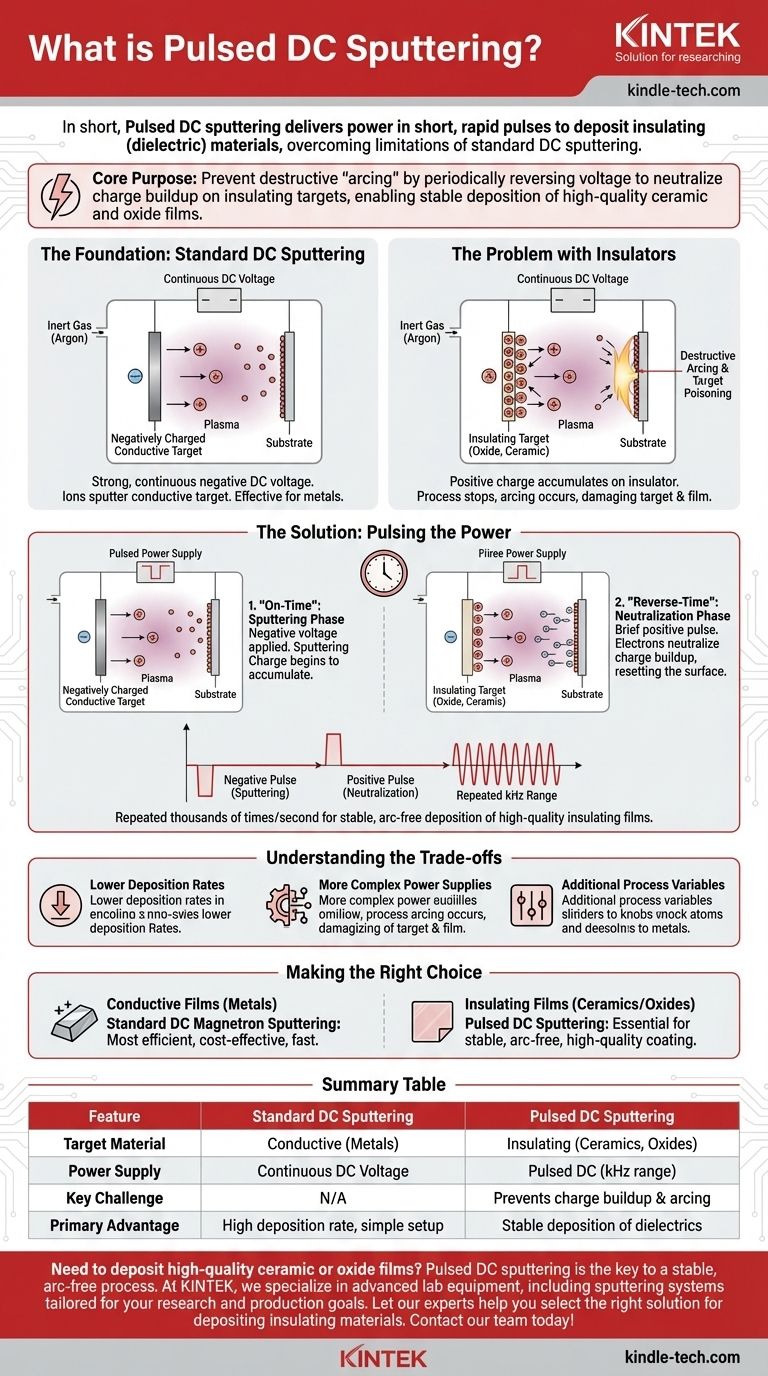
In short, pulsed DC sputtering is a thin-film deposition technique where the electrical power applied to the sputtering target is delivered in short, rapid pulses instead of a continuous stream. This method is specifically designed to overcome the critical challenge of sputtering insulating (dielectric) materials, which is not possible with standard direct current (DC) sputtering.
The core purpose of pulsed DC sputtering is to prevent a destructive electrical phenomenon known as "arcing." By periodically reversing the voltage on an insulating target, it neutralizes charge buildup that would otherwise stop the process, enabling the stable deposition of high-quality ceramic and oxide films.
The Foundation: Standard DC Sputtering
To understand pulsed DC, we must first look at the standard DC process. Sputtering is a vacuum deposition method for creating exceptionally thin coatings on a substrate.
How It Works
The process begins by placing the material to be coated (the substrate) and the coating material (the target) into a vacuum chamber. The chamber is filled with an inert gas, typically Argon.
A strong, continuous negative DC voltage is applied to the target. This high voltage ignites the Argon gas into a plasma, which is a cloud of positive Argon ions and free electrons.
The positively charged Argon ions are powerfully attracted to the negatively charged target. They accelerate and crash into the target's surface, physically knocking off, or "sputtering," atoms of the target material. These sputtered atoms then travel through the chamber and deposit onto the substrate, building up a thin film layer by layer.
The Problem Pulsed DC Was Built to Solve
Standard DC sputtering is highly effective and efficient, but it has one major limitation: it only works with electrically conductive targets, such as metals.
The Challenge of "Target Poisoning"
If you try to sputter an insulating material, like an oxide or a ceramic, a fundamental problem occurs. The positive Argon ions strike the target, but because the material is an insulator, their positive charge cannot dissipate.
This charge accumulates rapidly on the surface of the target.
The Consequence: Destructive Arcing
This layer of positive charge, known as "target poisoning," repels the incoming positive Argon ions. This effectively shuts down the sputtering process.
Worse, the immense electrical potential can build until it discharges uncontrollably in a powerful arc. These arcs can damage the target, the substrate, and the delicate film being deposited, rendering the process unstable and useless.
The Solution: Pulsing the Power
Pulsed DC sputtering solves the arcing problem with a simple but ingenious modification: it turns the power on and off in a controlled cycle.
The "On-Time": Sputtering Phase
For a short period, a negative voltage is applied to the target, and sputtering proceeds just as it does in the standard DC process. During this phase, positive charge begins to accumulate on the insulating target surface.
The "Reverse-Time": Neutralization Phase
Before the charge can build to a level that causes an arc, the power supply briefly switches the voltage to a slightly positive potential (or turns it off completely). This short positive pulse attracts the free electrons from the plasma to the target surface.
These electrons immediately neutralize the positive charge that built up during the on-time, effectively "resetting" the target surface.
The Result: Stable Deposition
By repeating this cycle tens of thousands of times per second (in the kilohertz range), pulsed DC sputtering prevents charge from ever accumulating to a dangerous level. This allows for the smooth, stable, and arc-free deposition of high-quality insulating films.
Understanding the Trade-offs
While it solves a critical problem, pulsed DC sputtering has considerations that differentiate it from other methods.
Lower Deposition Rates
Because the power is not active 100% of the time, the rate at which material is deposited is inherently lower than what could be achieved with a conductive target using standard DC sputtering.
More Complex Power Supplies
The hardware required to generate precise, high-frequency pulses is more sophisticated and costly than a simple, continuous DC power supply.
Additional Process Variables
The pulse frequency and duty cycle (the ratio of on-time to total cycle time) become critical process parameters that must be carefully optimized to achieve the desired film properties and deposition rate.
Making the Right Choice for Your Goal
Selecting the correct sputtering technique depends entirely on the material you intend to deposit.
- If your primary focus is depositing a conductive film (e.g., pure metals or alloys): Standard DC magnetron sputtering is the most efficient, cost-effective, and fastest method.
- If your primary focus is depositing an insulating or dielectric film (e.g., oxides, nitrides, or ceramics): Pulsed DC sputtering is the essential technique for achieving a stable, arc-free process and a high-quality final coating.
Ultimately, pulsed DC technology fundamentally expands the capabilities of sputtering, enabling the creation of advanced dielectric and ceramic thin films critical to modern electronics and optics.
Summary Table:
| Feature | Standard DC Sputtering | Pulsed DC Sputtering |
|---|---|---|
| Target Material | Conductive (Metals) | Insulating (Ceramics, Oxides) |
| Power Supply | Continuous DC Voltage | Pulsed DC (kHz range) |
| Key Challenge | N/A | Prevents charge buildup & arcing |
| Primary Advantage | High deposition rate, simple setup | Stable deposition of dielectrics |
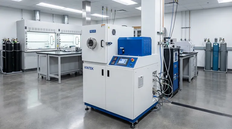
Need to deposit high-quality ceramic or oxide films? Pulsed DC sputtering is the key to a stable, arc-free process. At KINTEK, we specialize in advanced lab equipment, including sputtering systems tailored for your specific research and production goals. Let our experts help you select the right solution for depositing insulating materials. Contact our team today to discuss your thin-film deposition needs!
Visual Guide
Related Products
- Spark Plasma Sintering Furnace SPS Furnace
- Chemical Vapor Deposition CVD Equipment System Chamber Slide PECVD Tube Furnace with Liquid Gasifier PECVD Machine
People Also Ask
- What is the pressure for spark plasma sintering? A Guide to Optimizing SPS Parameters
- What are the fundamentals of spark plasma sintering process? Unlock Rapid, High-Performance Material Consolidation
- What is the process fundamentals of spark plasma sintering? Achieve Rapid, High-Density Material Consolidation
- What is SPS sintering method? A Guide to High-Speed, High-Performance Material Fabrication
- What technical advantages does a Spark Plasma Sintering (SPS) furnace offer for LZP ceramics? Enhance Ionic Conductivity

