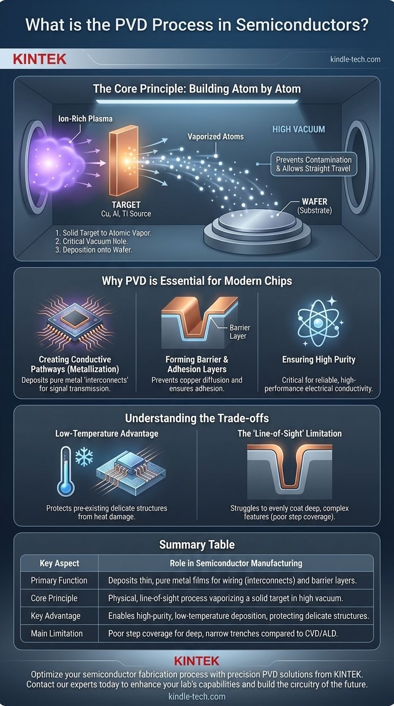
In semiconductor manufacturing, Physical Vapor Deposition (PVD) is a high-vacuum process used to deposit extremely thin, pure films of material onto a silicon wafer. It works by vaporizing a solid source material, known as a "target," and allowing its atoms to travel through the vacuum and condense onto the wafer's surface. This technique is fundamental for building the intricate conductive layers that form the wiring of a microchip.
PVD is not merely a coating technique; it is a precision engineering process for constructing the metallic circuitry inside an integrated circuit. It is the primary method used to create the highly pure, uniform metal layers—the "interconnects"—that carry signals between millions of transistors on a chip.
The Core Principle: Building Atom by Atom
PVD is a "line-of-sight" process that involves three primary steps inside a vacuum chamber. The precision of this method is what makes modern, high-performance electronics possible.
From Solid Target to Atomic Vapor
The process begins with a solid, high-purity slab of the desired material, called a target (e.g., copper, aluminum, titanium). Inside the vacuum, this target is bombarded with a high-energy source, most commonly an ion-rich plasma. This bombardment physically knocks atoms loose from the target, transforming the solid material into a vapor.
The Critical Role of the Vacuum
The entire process occurs under a very high vacuum. This is essential for two reasons. First, it prevents contamination by removing air molecules like oxygen and nitrogen that would otherwise react with the vaporized metal. Second, the lack of air allows the vaporized atoms to travel in a straight line directly to the wafer without colliding with other particles.
Deposition onto the Wafer
The vaporized atoms travel through the chamber and strike the cooler silicon wafer, which acts as the substrate. Upon hitting the wafer's surface, they condense back into a solid state, forming a thin, uniform, and highly pure film. This atom-by-atom buildup allows for exceptional control over the film's thickness and properties.
Why PVD is Essential for Modern Chips
While PVD is used in many industries, its application in semiconductor fabrication is uniquely critical. It is not used for decoration but for creating essential electronic functions.
Creating Conductive Pathways (Metallization)
The most important role of PVD in chipmaking is metallization. It is the go-to process for depositing the metal layers (typically aluminum or copper) that serve as the microscopic "wires" connecting transistors and other components. These pathways are known as interconnects, and their quality directly impacts the chip's speed and reliability.
Forming Barrier and Adhesion Layers
Modern chips often use copper for interconnects, but copper atoms can diffuse into the surrounding silicon, destroying the device. To prevent this, a very thin barrier layer (e.g., tantalum or titanium nitride) is first deposited using PVD. This layer acts as a wall, containing the copper while also helping it adhere properly to the wafer's surface.
Ensuring High Purity
The electrical performance of a wire is highly sensitive to impurities. The high-vacuum environment of PVD ensures the deposited metal films are exceptionally pure. This purity is non-negotiable for producing reliable chips that perform to specification.
Understanding the Trade-offs
No single process is perfect for every application. Understanding the limitations of PVD is key to appreciating its role alongside other fabrication techniques.
The "Line-of-Sight" Limitation
Because PVD atoms travel in straight lines, the process struggles to evenly coat the bottom and sidewalls of deep, narrow trenches on a chip. This issue, known as poor step coverage, becomes more significant as chip features shrink. The top "shoulders" of a trench get a thick coating while the bottom gets very little.
The Low-Temperature Advantage
The PVD process occurs at relatively low temperatures. This is a major advantage in semiconductor manufacturing, as it prevents damage to the delicate transistor structures that have already been built on the wafer in previous steps. High temperatures could alter or destroy these intricate components.
Complementary Deposition Methods
For the most advanced chip designs with complex 3D structures, the line-of-sight limitation of PVD can be a deal-breaker. In these cases, other techniques like Chemical Vapor Deposition (CVD) or Atomic Layer Deposition (ALD) are used. These methods are chemical rather than physical and excel at creating perfectly uniform "conformal" coatings over any shape.
Making the Right Choice for Your Goal
PVD is a cornerstone of semiconductor fabrication, but its application is specific. Its value depends on the manufacturing goal.
- If your primary focus is backend-of-line (BEOL) wiring: PVD is the foundational technology for depositing the pure metal interconnects and the critical barrier layers that make them possible.
- If your primary focus is creating insulating films: You would typically look to Chemical Vapor Deposition (CVD), which is better suited for depositing oxide and nitride dielectrics.
- If your primary focus is coating highly complex 3D features: You would select Atomic Layer Deposition (ALD) for its unmatched ability to create perfectly uniform films, even inside the deepest trenches.
Ultimately, understanding PVD is to understand how the microscopic wiring of the digital world is meticulously built, one atom at a time.
Summary Table:
| Key Aspect | Role in Semiconductor Manufacturing |
|---|---|
| Primary Function | Deposits thin, pure metal films for conductive wiring (interconnects) and barrier layers. |
| Core Principle | A physical, line-of-sight process that vaporizes a solid target material in a high vacuum. |
| Key Advantage | Enables high-purity, low-temperature deposition, protecting delicate transistor structures. |
| Main Limitation | Poor step coverage for coating deep, narrow trenches compared to CVD or ALD. |
Optimize your semiconductor fabrication process with precision PVD solutions from KINTEK.
As a leading provider of high-performance lab equipment and consumables, KINTEK specializes in the tools and materials essential for advanced semiconductor manufacturing. Whether you are developing next-generation microchips or refining your production line, our expertise in PVD targets and related consumables ensures you achieve the high-purity, uniform films required for reliable, high-speed electronics.
Contact our experts today to discuss how our solutions can enhance your lab's capabilities and help you build the intricate circuitry of the future.
Visual Guide
Related Products
- Inclined Rotary Plasma Enhanced Chemical Vapor Deposition PECVD Equipment Tube Furnace Machine
- HFCVD Machine System Equipment for Drawing Die Nano-Diamond Coating
- Chemical Vapor Deposition CVD Equipment System Chamber Slide PECVD Tube Furnace with Liquid Gasifier PECVD Machine
- 915MHz MPCVD Diamond Machine Microwave Plasma Chemical Vapor Deposition System Reactor
- CVD Diamond Domes for Industrial and Scientific Applications
People Also Ask
- What is PECVD silicon deposition? Achieve Low-Temperature, High-Quality Thin Films
- What is the difference between CVD and PECVD? Choose the Right Thin-Film Deposition Method
- What is plasma enhanced chemical vapour deposition process? Unlock Low-Temperature, High-Quality Thin Films
- What is meant by vapor deposition? A Guide to Atomic-Level Coating Technology
- What is plasma enhanced chemical vapor deposition? Achieve Low-Temperature, High-Quality Thin Films