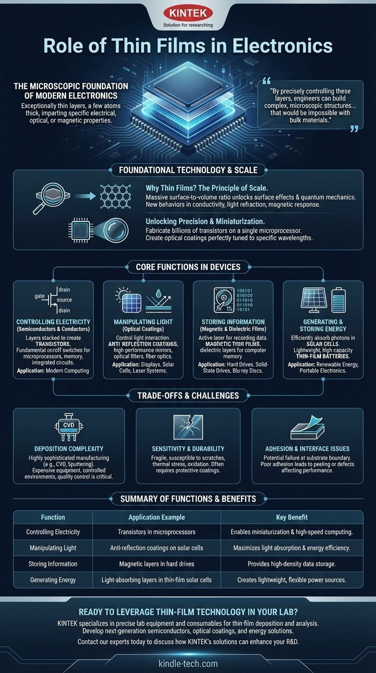
In essence, thin films are the microscopic foundation of modern electronics. They are exceptionally thin layers of material, often just a few atoms thick, deposited onto a surface to impart specific electrical, optical, or magnetic properties. This technology is the key enabler for the miniaturization, power, and efficiency we expect from devices ranging from computer processors to solar panels.
The central role of a thin film is to leverage the unique physical properties that materials exhibit at near-atomic scales. By precisely controlling these layers, engineers can build complex, microscopic structures that conduct electricity, manipulate light, or store information in ways that would be impossible with bulk materials.
Why Thin Films are a Foundational Technology
To understand the role of thin films, you must first grasp why they are so different from standard materials. The answer lies in the physics of scale.
The Principle of Scale
When a material is reduced to a "thin film" with a thickness measured in nanometers, its properties change dramatically. This is primarily due to a massive increase in its surface-to-volume ratio.
At this scale, surface effects and quantum mechanics begin to dominate over the properties of the bulk material, unlocking new behaviors in conductivity, light refraction, and magnetic response.
Unlocking Precision and Miniaturization
This ability to engineer material properties at the atomic level is the core reason thin films are indispensable. They allow for the construction of incredibly complex and small components.
This precision is what enables the fabrication of billions of transistors on a single microprocessor or the creation of optical coatings that are perfectly tuned to a specific wavelength of light.
Core Functions of Thin Films in Devices
While the applications are vast, the function of a thin film in an electronic device typically falls into one of several key categories.
Controlling Electricity (Semiconductors & Conductors)
This is the most critical role in microelectronics. Layers of semiconductor, conducting, and insulating thin films are stacked to create transistors.
These transistors are the fundamental on/off switches that form the basis of all microprocessors, memory chips, and integrated circuits, making modern computing possible.
Manipulating Light (Optical Coatings)
Thin films are crucial for controlling how light interacts with a device's surface. They are used as anti-reflection coatings on display panels and solar cells to maximize light transmission or absorption.
They also form the basis for high-performance mirrors, optical filters, and coatings on fiber optics that improve the performance of communication networks and laser systems.
Storing Information (Magnetic & Dielectric Films)
In data storage, thin films serve as the active layer for recording information. In hard drives, for example, layers of magnetic thin films are used to store data as magnetic bits.
They are also used as protective coatings on optical data storage devices like Blu-ray discs and as the dielectric layers in advanced forms of computer memory.
Generating and Storing Energy
Thin films are essential for renewable energy. In solar cells, specific thin-film layers are designed to efficiently absorb photons from sunlight and convert them into electrical power.
Similarly, thin-film batteries utilize ultra-thin layers of electrolytes and electrode materials to create lightweight, flexible, and high-capacity power sources for portable electronics.
Understanding the Trade-offs and Challenges
While powerful, thin-film technology is not without its complexities. Acknowledging these limitations is crucial for understanding its application.
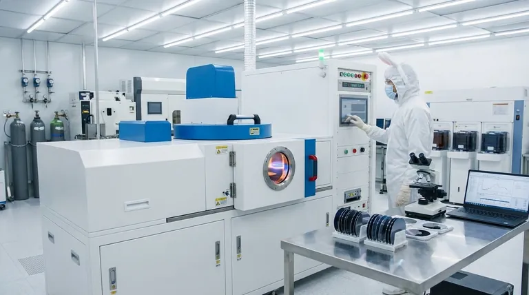
Complexity of Deposition
Creating a perfectly uniform, defect-free thin film is a highly sophisticated manufacturing process. Techniques like chemical vapor deposition (CVD) or sputtering require expensive equipment and meticulously controlled environments.
Any imperfection in the film's thickness or composition can lead to device failure, making quality control a significant challenge.
Sensitivity and Durability
By their very nature, thin films are fragile. Their extreme thinness makes them susceptible to physical scratches, damage from thermal stress, or degradation from environmental factors like oxidation.
Protecting these delicate layers is a primary concern in device design, often requiring additional protective coatings.
Adhesion and Interface Issues
The boundary where the thin film meets the underlying material (the substrate) is a critical point of potential failure. Poor adhesion can cause the film to peel or delaminate.
Furthermore, interactions at this interface can create electrical or chemical defects that compromise the performance of the entire device.
How Thin Films Define Device Capabilities
To apply this knowledge, consider how the function of a thin film directly enables the primary goal of a given technology.
- If your primary focus is computational power: The role of thin films is to create the billions of microscopic transistors that form the logic gates inside a microprocessor.
- If your primary focus is energy efficiency: Thin films are engineered to maximize light absorption in solar cells or enable the creation of lightweight, high-density batteries.
- If your primary focus is data storage: Thin films provide the essential magnetic or phase-change layers for high-density memory in hard drives and solid-state drives.
- If your primary focus is visual displays: The clarity and color of modern screens depend on thin-film layers that filter light, reduce reflection, and form the pixel arrays.
Ultimately, understanding the role of thin films is to recognize the fundamental principle of material science that makes modern high-performance electronics possible.
Summary Table:
| Function | Application Example | Key Benefit |
|---|---|---|
| Controlling Electricity | Transistors in microprocessors | Enables miniaturization and high-speed computing |
| Manipulating Light | Anti-reflection coatings on solar cells | Maximizes light absorption and energy efficiency |
| Storing Information | Magnetic layers in hard drives | Provides high-density data storage |
| Generating Energy | Light-absorbing layers in thin-film solar cells | Creates lightweight, flexible power sources |
Ready to leverage thin-film technology in your lab?
Thin films are the cornerstone of advanced electronics, enabling the high-performance devices that power modern research and innovation. At KINTEK, we specialize in providing the precise lab equipment and consumables needed for thin-film deposition and analysis.
Whether you are developing next-generation semiconductors, optical coatings, or energy storage solutions, our expertise can help you achieve superior results. Our range of products supports the meticulous processes required for creating defect-free, high-performance thin films.
Contact our experts today to discuss how KINTEK's solutions can enhance your thin-film research and development, ensuring precision, reliability, and breakthrough performance in your laboratory.
Visual Guide
Related Products
- Tungsten Evaporation Boat for Thin Film Deposition
- Aluminum-Plastic Flexible Packaging Film for Lithium Battery Packaging
- Thin-Layer Spectral Electrolysis Electrochemical Cell
- Lab Plastic PVC Calender Stretch Film Casting Machine for Film Testing
People Also Ask
- What is the source of evaporation for thin film? Choosing Between Thermal and E-Beam Methods
- What methods are used to deposit thin films? A Guide to PVD, CVD, and ALD Techniques
- What are the types of thin film? A Guide to PVD vs. CVD Deposition Methods
- What are the two primary categories of deposition technologies? PVD vs. CVD Explained
- What is the difference between PVD and CVD? Choose the Right Thin-Film Deposition Technique


