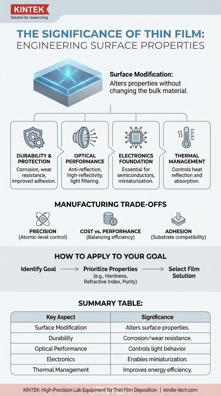
In essence, the significance of thin film lies in its ability to dramatically alter the surface properties of a material without changing the material itself. These microscopic layers, often just a few atoms thick, can provide enhanced durability, resistance to corrosion, and create entirely new optical or electrical functionalities. This makes them a cornerstone of modern technology, from consumer electronics to advanced scientific instruments.
A thin film is not just a simple coating; it is a precisely engineered layer that unlocks properties a bulk material could never possess on its own. Its significance comes from enabling this high degree of surface-level customization across countless industries.
Beyond a Simple Coating: Engineering New Functionality
The true power of thin film technology is its versatility. By depositing a carefully selected material onto a substrate, we can imbue that substrate with entirely new, desirable characteristics.
The Principle of Surface Modification
A thin film is a layer of material ranging from nanometers to several micrometers in thickness. The core principle is that this ultra-thin layer dictates how the object's surface interacts with the outside world, whether that interaction involves light, electricity, heat, or physical contact.
Enhancing Durability and Resistance
One of the most common applications is for protection. A thin film can act as a hard, durable shield on a component.
This provides critical benefits like corrosion resistance, wear resistance, and improved adhesion for subsequent layers, extending the lifespan and reliability of the underlying part.
Manipulating Light and Energy
Thin films are fundamental to modern optics. By controlling the thickness and refractive index of the film, we can precisely manage how light behaves.
This enables anti-reflection coatings on eyeglasses and solar panels, high-reflectivity coatings for lasers and mirrors, and infrared-reflecting coatings that improve the efficiency of filament lamps by keeping heat inside. They are also used to prevent heat from passing through window glass.
Driving the Future of Electronics
Thin films are the foundation of the semiconductor industry. Integrated circuits are built by depositing a sequence of thin films onto a silicon wafer to create transistors and pathways for electricity.
As devices shrink, the quality and precision of these films become paramount. A defect of even a few misplaced atoms in a thin film can ruin the performance of a computer chip, making high-precision deposition essential for continued miniaturization.
Understanding the Manufacturing Trade-offs
While the benefits are immense, producing a high-quality thin film is a complex engineering challenge that involves balancing competing priorities.
The Challenge of Precision
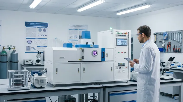
Depositing a uniform layer that is only a few molecules thick requires highly specialized and expensive equipment. Achieving this precision consistently is a major focus of quality control in manufacturing.
Balancing Cost and Performance
The choice of material and deposition method directly impacts the final cost. A simple protective coating may be relatively inexpensive, while a multi-layer optical filter for a specific scientific purpose requires a much more complex and costly process. Efficiency and client specifications are always key considerations.
Adhesion and Substrate Compatibility
A thin film is only useful if it adheres perfectly to the substrate. Ensuring strong, long-lasting adhesion is a critical factor that influences material selection for both the film and the base material.
How to Apply This to Your Goal
The "best" thin film solution is entirely dependent on the problem you are trying to solve.
- If your primary focus is mechanical protection: You will prioritize films that offer high hardness, corrosion resistance, and strong adhesion.
- If your primary focus is optical performance: Your choice will be dictated by the desired refractive index, reflectivity, or light filtering properties.
- If your primary focus is advanced electronics: You must demand films with extreme purity, atomic-level uniformity, and precise electrical characteristics.
- If your primary focus is thermal management: You will need films designed specifically to reflect or absorb certain wavelengths of heat energy.
By mastering the art of the incredibly small, thin film technology enables us to solve some of the world's biggest engineering challenges.
Summary Table:
| Key Aspect | Significance of Thin Film |
|---|---|
| Surface Modification | Alters surface properties without changing the bulk material. |
| Durability & Protection | Provides corrosion resistance, wear resistance, and improved adhesion. |
| Optical Performance | Enables anti-reflection, high-reflectivity coatings, and light filtering. |
| Electronics Foundation | Essential for semiconductor manufacturing and device miniaturization. |
| Thermal Management | Controls heat reflection and absorption for improved energy efficiency. |
Ready to engineer the perfect surface properties for your project?
At KINTEK, we specialize in providing high-precision lab equipment and consumables for thin film deposition. Whether your goal is enhancing durability, achieving specific optical performance, or developing advanced electronic components, our solutions are designed to meet the exacting demands of modern thin film technology.
Let our expertise help you master the art of the incredibly small. Contact our specialists today to discuss your specific application and discover how KINTEK can support your laboratory's innovation in surface science.
Visual Guide
Related Products
- Aluminized Ceramic Evaporation Boat for Thin Film Deposition
- Tungsten Evaporation Boat for Thin Film Deposition
- Electron Beam Evaporation Coating Oxygen-Free Copper Crucible and Evaporation Boat
- Molybdenum Tungsten Tantalum Evaporation Boat for High Temperature Applications
- Aluminum-Plastic Flexible Packaging Film for Lithium Battery Packaging
People Also Ask
- What are the alternatives to sputtering? Choose the Right Thin Film Deposition Method
- Why is an alumina boat selected for catalyst precursors? Ensure Sample Purity at 1000 °C
- What is the source of evaporation for thin film? Choosing Between Thermal and E-Beam Methods
- Why are high-purity ceramic boats used for lignin activation? Ensure Purity & Thermal Stability
- What is thin film deposition? Unlock Advanced Surface Engineering for Your Materials


