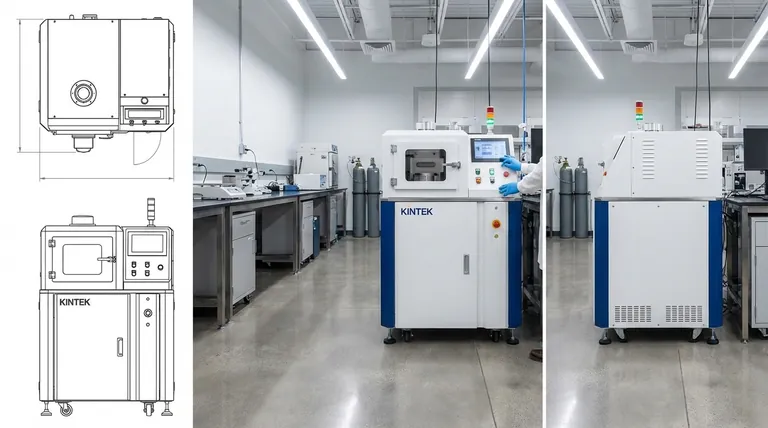
In essence, sputtering is a highly controlled physical vapor deposition (PVD) method used to create ultra-thin films. The process works by bombarding a solid source material, known as a "target," with energetic ions in a vacuum. This bombardment physically knocks atoms loose from the target, which then travel and deposit onto a nearby surface, or "substrate," forming a precise and uniform coating.
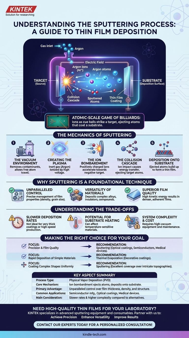
Sputtering is best understood as an atomic-scale game of billiards. In a vacuum, ions are used as cue balls to strike a target, ejecting atoms that then coat a substrate. This method's power lies in its exceptional control over the final film's thickness, density, and structure.
The Mechanics of the Sputtering Process
To grasp why sputtering is so widely used in industries from semiconductor manufacturing to optics, it's essential to understand its core mechanics. The entire process unfolds in a sequence of carefully controlled steps inside a vacuum chamber.
The Vacuum Environment
The process must occur in a high vacuum. This serves two critical purposes: it removes atmospheric gases that could contaminate the film, and it allows the sputtered atoms to travel freely from the target to the substrate without colliding with other particles.
Creating the Plasma
An inert gas, most commonly Argon, is introduced into the chamber. A high voltage is then applied, creating a strong electric field between the target (which acts as the cathode, or negative terminal) and the substrate. This field energizes the gas, stripping electrons from the Argon atoms and creating a glowing, ionized gas known as a plasma.
The Ion Bombardment
The positively charged Argon ions within the plasma are now strongly attracted to the negatively charged target. They accelerate toward the target at high velocity, driven by the electric field.
The Collision Cascade
When an energetic ion strikes the target, it doesn't just chip off a single atom. Instead, it transfers its momentum in a chain reaction beneath the target's surface, known as a collision cascade. When this cascade of energy reaches the surface, it overcomes the forces holding the atoms together, ejecting target atoms into the chamber.
Deposition onto the Substrate
These ejected, or "sputtered," atoms travel through the vacuum and land on the substrate. Over time, these atoms build up, nucleating and growing into a thin, solid film with highly specific properties.
Why Sputtering is a Foundational Technique
Sputtering is not just one method among many; its unique characteristics make it indispensable for creating high-performance materials.
Unparalleled Control
The primary advantage of sputtering is control. By precisely managing factors like gas pressure, voltage, and temperature, engineers can dictate a film's properties, including its density, grain size, orientation, and electrical resistivity.
Versatility of Materials
Unlike some other deposition methods that rely on melting and evaporating materials, sputtering is a purely physical process. This allows it to deposit a vast range of materials, including complex alloys, insulators, and compounds that would decompose if heated.
Superior Film Quality
Sputtered atoms arrive at the substrate with significantly more kinetic energy than evaporated atoms. This energy results in denser, more adherent films with better coverage over complex, non-flat surfaces.
Understanding the Trade-offs
No technique is perfect. To use sputtering effectively, you must be aware of its inherent limitations.
Slower Deposition Rates
Generally, sputtering is a slower process compared to techniques like thermal evaporation. This can make it less suitable for applications requiring very thick coatings or high-speed production.
Potential for Substrate Heating
The energy transfer from the plasma and depositing atoms can heat the substrate. This can be problematic when coating temperature-sensitive materials like certain plastics or biological samples.
System Complexity and Cost
Sputtering systems are sophisticated pieces of equipment involving high-vacuum pumps and precise power supplies. This complexity translates to a higher initial investment and more demanding maintenance compared to simpler methods.
Making the Right Choice for Your Goal
Selecting a deposition method depends entirely on the desired outcome. Sputtering offers precision at the cost of speed and complexity.
- If your primary focus is precision and film quality: Sputtering offers superior control over film properties, making it ideal for high-performance optical coatings, semiconductors, and medical devices.
- If your primary focus is rapid deposition of simple materials: A technique like thermal evaporation may be a more efficient and cost-effective choice for less demanding applications like decorative coatings.
- If your primary focus is coating complex shapes uniformly: Sputtering provides excellent coverage over intricate topographies, ensuring a consistent film where line-of-sight methods would fail.
Understanding these core principles allows you to leverage sputtering not just as a process, but as a precise tool for engineering materials at the atomic level.
Summary Table:
| Key Aspect | Description |
|---|---|
| Process Type | Physical Vapor Deposition (PVD) |
| Core Mechanism | Ion bombardment of a target material ejects atoms, which deposit onto a substrate. |
| Primary Advantage | Unparalleled control over film thickness, density, and structure. |
| Common Applications | Semiconductor manufacturing, optical coatings, medical devices. |
| Main Consideration | Slower deposition rates and higher system complexity compared to some alternatives. |
Need High-Quality Thin Films for Your Laboratory?
KINTEK specializes in providing advanced sputtering equipment and consumables to meet the precise demands of modern laboratories. Whether you are developing next-generation semiconductors, durable optical coatings, or innovative medical devices, our solutions deliver the control and film quality you require.
Partner with KINTEK to:
- Achieve Precision: Create ultra-thin films with exact thickness, density, and composition.
- Enhance Versatility: Deposit a wide range of materials, including complex alloys and compounds.
- Improve Results: Benefit from superior film adhesion and coverage on complex surfaces.
Let our expertise in lab equipment help you engineer materials at the atomic level. Contact our experts today for a personalized consultation!
Visual Guide
Related Products
- Spark Plasma Sintering Furnace SPS Furnace
- Vacuum Induction Melting Spinning System Arc Melting Furnace
- Chemical Vapor Deposition CVD Equipment System Chamber Slide PECVD Tube Furnace with Liquid Gasifier PECVD Machine
- Customer Made Versatile CVD Tube Furnace Chemical Vapor Deposition Chamber System Equipment
People Also Ask
- Why are Spark Plasma Sintering (SPS) furnaces or hot presses utilized in the preparation of Li3PS4 solid electrolytes?
- What is the mechanism of SPS process? A Deep Dive into Rapid, Low-Temperature Sintering
- What is the process fundamentals of spark plasma sintering? Achieve Rapid, High-Density Material Consolidation
- What are the fundamentals of spark plasma sintering process? Unlock Rapid, High-Performance Material Consolidation
- What are the advantages of CAMI/SPS for W-Cu composite preparation? Reduce cycles from hours to seconds.


