Knowledge What is the substrate material for thin film deposition? A Guide to Selecting the Right Foundation
Author avatar

Tech Team · Kintek Solution

Updated 1 week ago

What is the substrate material for thin film deposition? A Guide to Selecting the Right Foundation

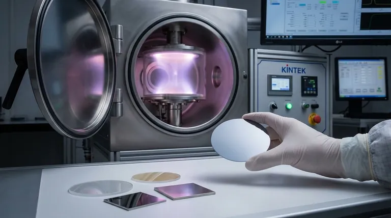
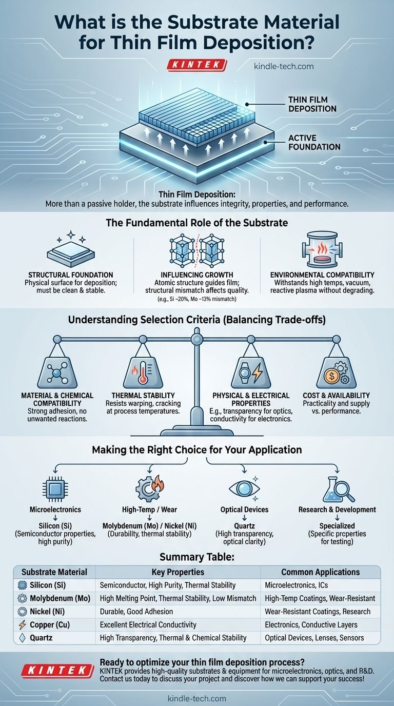
In thin film deposition, the substrate is the foundational material or surface onto which a new layer of material is grown or deposited. While many materials can serve this purpose, the most common choices for advanced applications include silicon (Si), molybdenum (Mo), nickel (Ni), copper (Cu), and quartz, each selected for its specific properties. The choice of substrate is as critical as the choice of the film material itself.

The substrate is not merely a passive holder for the thin film. It is an active component in the deposition system that directly influences the film's structural integrity, properties, and ultimate performance in its intended application.

The Fundamental Role of the Substrate

Understanding the function of the substrate moves beyond seeing it as a simple base. It is an integral part of the final engineered product, dictating what is possible during and after deposition.

Providing the Structural Foundation

The substrate provides the physical surface where the deposition process, whether chemical or physical, takes place. It must be clean, stable, and often precisely engineered to serve as a template for the film.

Influencing Film Growth and Structure

The atomic arrangement of the substrate's surface can guide the growth of the thin film. A key factor is structural mismatch, or the difference in the crystalline lattice spacing between the substrate and the film material.

For example, silicon has a ~20% structural mismatch with certain film materials, while molybdenum has a ~13% mismatch. This difference can introduce stress and defects, affecting the film's quality.

Compatibility with the Deposition Environment

Deposition processes like Chemical Vapor Deposition (CVD) and Physical Vapor Deposition (PVD) often involve extreme conditions. The substrate must be able to withstand high temperatures, vacuum environments, and potentially reactive plasmas without degrading.

Understanding the Selection Criteria

Selecting the correct substrate is a process of balancing trade-offs. No single material is perfect for every situation; the choice depends on a careful analysis of multiple interacting factors.

Material and Chemical Compatibility

The thin film must adhere strongly to the substrate. This requires chemical compatibility, ensuring that the film material bonds to the substrate surface without unwanted reactions that could compromise the interface.

Thermal Stability

Many deposition techniques use thermal energy from resistive heaters or infrared lamps to drive the reaction. The substrate must have a melting point and thermal expansion coefficient suitable for the process temperatures to prevent warping, cracking, or delamination.

Physical and Electrical Properties

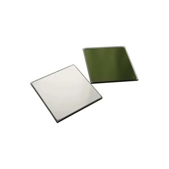
The substrate's own properties are critical for the final device's function. For optical applications, a transparent substrate like quartz is necessary. For electronics, the exceptional purity and semiconductor properties of silicon wafers are indispensable.

Cost and Availability

Practical considerations are always a factor. Materials like silicon are widely available in high purity due to their dominance in the semiconductor industry, making them a cost-effective choice for many applications. More exotic substrates may offer superior performance but at a significantly higher cost.

Making the Right Choice for Your Application

The optimal substrate is determined by the primary goal of your project. The material you deposit onto is as important as the material you are depositing.

  • If your primary focus is microelectronics: Silicon (Si) is the default choice due to its well-understood semiconductor properties, high purity, and established manufacturing ecosystem.
  • If your primary focus is high-temperature or wear-resistant coatings: A metallic substrate like molybdenum (Mo) or nickel (Ni) may be chosen for its durability and thermal stability.
  • If your primary focus is optical devices: A transparent material with excellent optical clarity, such as quartz or specialized glass, is the required foundation.
  • If your primary focus is research and development: The choice will be driven by the specific properties you wish to induce in the film, often leading to less common substrates to test material interactions.

Ultimately, selecting the right substrate is the first step in engineering the performance of the final product.

Summary Table:

Substrate Material Key Properties Common Applications
Silicon (Si) Semiconductor properties, high purity, thermal stability Microelectronics, integrated circuits
Molybdenum (Mo) High melting point, thermal stability, low structural mismatch High-temperature coatings, wear-resistant layers
Nickel (Ni) Durable, good adhesion for many films Wear-resistant coatings, research
Copper (Cu) Excellent electrical conductivity Electronics, conductive layers
Quartz High transparency, thermal and chemical stability Optical devices, lenses, sensors

Ready to optimize your thin film deposition process? The right substrate is critical for your film's performance, whether for microelectronics, optics, or R&D. KINTEK specializes in providing high-quality lab equipment and consumables, including substrates and deposition systems, to meet your specific laboratory needs. Our experts can help you select the perfect materials to ensure strong adhesion, thermal stability, and superior results. Contact us today to discuss your project and discover how we can support your success!

Related Products

People Also Ask

Related Products

Inclined Rotary Plasma Enhanced Chemical Vapor Deposition PECVD Equipment Tube Furnace Machine

Inclined Rotary Plasma Enhanced Chemical Vapor Deposition PECVD Equipment Tube Furnace Machine

Upgrade your coating process with PECVD coating equipment. Ideal for LED, power semiconductors, MEMS and more. Deposits high-quality solid films at low temps.

RF PECVD System Radio Frequency Plasma-Enhanced Chemical Vapor Deposition RF PECVD

RF PECVD System Radio Frequency Plasma-Enhanced Chemical Vapor Deposition RF PECVD

RF-PECVD is an acronym for "Radio Frequency Plasma-Enhanced Chemical Vapor Deposition." It deposits DLC (Diamond-like carbon film) on germanium and silicon substrates. It is utilized in the 3-12um infrared wavelength range.

Chemical Vapor Deposition CVD Equipment System Chamber Slide PECVD Tube Furnace with Liquid Gasifier PECVD Machine

Chemical Vapor Deposition CVD Equipment System Chamber Slide PECVD Tube Furnace with Liquid Gasifier PECVD Machine

KT-PE12 Slide PECVD System: Wide power range, programmable temp control, fast heating/cooling with sliding system, MFC mass flow control & vacuum pump.

MgF2 Magnesium Fluoride Crystal Substrate Window for Optical Applications

MgF2 Magnesium Fluoride Crystal Substrate Window for Optical Applications

Magnesium fluoride (MgF2) is a tetragonal crystal that exhibits anisotropy, making it imperative to treat it as a single crystal when engaging in precision imaging and signal transmission.

Customer Made Versatile CVD Tube Furnace Chemical Vapor Deposition Chamber System Equipment

Customer Made Versatile CVD Tube Furnace Chemical Vapor Deposition Chamber System Equipment

Get your exclusive CVD furnace with KT-CTF16 Customer Made Versatile Furnace. Customizable sliding, rotating, and tilting functions for precise reactions. Order now!

CVD Diamond Cutting Tool Blanks for Precision Machining

CVD Diamond Cutting Tool Blanks for Precision Machining

CVD Diamond Cutting Tools: Superior Wear Resistance, Low Friction, High Thermal Conductivity for Non-Ferrous Materials, Ceramics, Composites Machining

Microwave Plasma Chemical Vapor Deposition MPCVD Machine System Reactor for Lab and Diamond Growth

Microwave Plasma Chemical Vapor Deposition MPCVD Machine System Reactor for Lab and Diamond Growth

Get high-quality diamond films with our Bell-jar Resonator MPCVD machine designed for lab and diamond growth. Discover how Microwave Plasma Chemical Vapor Deposition works for growing diamonds using carbon gas and plasma.

Optical Window Glass Substrate Wafer Quartz Plate JGS1 JGS2 JGS3

Optical Window Glass Substrate Wafer Quartz Plate JGS1 JGS2 JGS3

The quartz plate is a transparent, durable, and versatile component widely used in various industries. Made from high-purity quartz crystal, it exhibits excellent thermal and chemical resistance.

CVD Diamond Domes for Industrial and Scientific Applications

CVD Diamond Domes for Industrial and Scientific Applications

Discover CVD diamond domes, the ultimate solution for high-performance loudspeakers. Made with DC Arc Plasma Jet technology, these domes deliver exceptional sound quality, durability, and power handling.

Split Chamber CVD Tube Furnace with Vacuum Station Chemical Vapor Deposition System Equipment Machine

Split Chamber CVD Tube Furnace with Vacuum Station Chemical Vapor Deposition System Equipment Machine

Efficient split chamber CVD furnace with vacuum station for intuitive sample checking and quick cooling. Up to 1200℃ max temperature with accurate MFC mass flowmeter control.

Cylindrical Resonator MPCVD Machine System Reactor for Microwave Plasma Chemical Vapor Deposition and Lab Diamond Growth

Cylindrical Resonator MPCVD Machine System Reactor for Microwave Plasma Chemical Vapor Deposition and Lab Diamond Growth

Learn about Cylindrical Resonator MPCVD Machine, the microwave plasma chemical vapor deposition method used for growing diamond gemstones and films in the jewelry and semi-conductor industries. Discover its cost-effective advantages over traditional HPHT methods.

Float Soda-Lime Optical Glass for Laboratory Use

Float Soda-Lime Optical Glass for Laboratory Use

Soda-lime glass, widely favored as an insulating substrate for thin/thick film deposition, is created by floating molten glass on molten tin. This method ensures uniform thickness and exceptionally flat surfaces.

Custom PTFE Teflon Parts Manufacturer for Sampling Solution Sample and Dry Powder Spoons

Custom PTFE Teflon Parts Manufacturer for Sampling Solution Sample and Dry Powder Spoons

The PTFE sampling spoon, also known as a solution spoon or sample spoon, is a crucial tool for accurately introducing dry powder samples in various analytical processes. Made from PTFE, these spoons offer excellent chemical stability, corrosion resistance, and non-stick properties, making them ideal for handling delicate and reactive substances in laboratory settings.

Polygon Press Mold for Lab

Polygon Press Mold for Lab

Discover precision polygon press molds for sintering. Ideal for pentagon-shaped parts, our molds ensure uniform pressure and stability. Perfect for repeatable, high-quality production.

High Purity Zinc Foil for Battery Lab Applications

High Purity Zinc Foil for Battery Lab Applications

There are very few harmful impurities in the chemical composition of zinc foil, and the surface of the product is straight and smooth; it has good comprehensive properties, processability, electroplating colorability, oxidation resistance and corrosion resistance, etc.

Square Bidirectional Pressure Mold for Lab Use

Square Bidirectional Pressure Mold for Lab Use

Discover precision in molding with our Square Bidirectional Pressure Mold. Ideal for creating diverse shapes and sizes, from squares to hexagons, under high pressure and uniform heating. Perfect for advanced material processing.

1200℃ Split Tube Furnace with Quartz Tube Laboratory Tubular Furnace

1200℃ Split Tube Furnace with Quartz Tube Laboratory Tubular Furnace

KT-TF12 split tube furnace: high-purity insulation, embedded heating wire coils, and max. 1200C. Widely used for new materials and chemical vapour deposition.

Custom PTFE Teflon Parts Manufacturer for Magnetic Stirring Bar

Custom PTFE Teflon Parts Manufacturer for Magnetic Stirring Bar

The PTFE magnetic stirring bar, made from high-quality PTFE, offers exceptional resistance to acids, alkalis, and organic solvents, coupled with high-temperature stability and low friction. Ideal for laboratory use, these stirring bars are compatible with standard flask ports, ensuring stability and safety during operations.

High-Purity Titanium Foil and Sheet for Industrial Applications

High-Purity Titanium Foil and Sheet for Industrial Applications

Titanium is chemically stable, with a density of 4.51g/cm3, which is higher than aluminum and lower than steel, copper, and nickel, but its specific strength ranks first among metals.

Custom PTFE Teflon Parts Manufacturer for PTFE Buchner Funnel and Triangular Funnel

Custom PTFE Teflon Parts Manufacturer for PTFE Buchner Funnel and Triangular Funnel

The PTFE funnel is a piece of laboratory equipment used primarily for filtration processes, particularly in the separation of solid and liquid phases in a mixture. This setup allows for efficient and rapid filtration, making it indispensable in various chemical and biological applications.


Leave Your Message