In essence, sputter deposition is a physical coating process akin to atomic-scale sandblasting. It uses high-energy ions to knock individual atoms off a source material, which then travel through a vacuum and deposit onto a separate surface, building up an ultra-thin, highly controlled film layer by layer. This method belongs to a broader category of techniques known as Physical Vapor Deposition (PVD).
To create high-quality thin films from virtually any material, engineers need a process that doesn't rely on melting or chemical reactions. Sputter deposition solves this by using energetic ion bombardment to physically eject atoms from a source, offering unparalleled control and versatility for depositing complex alloys, ceramics, and high-melting-point metals.

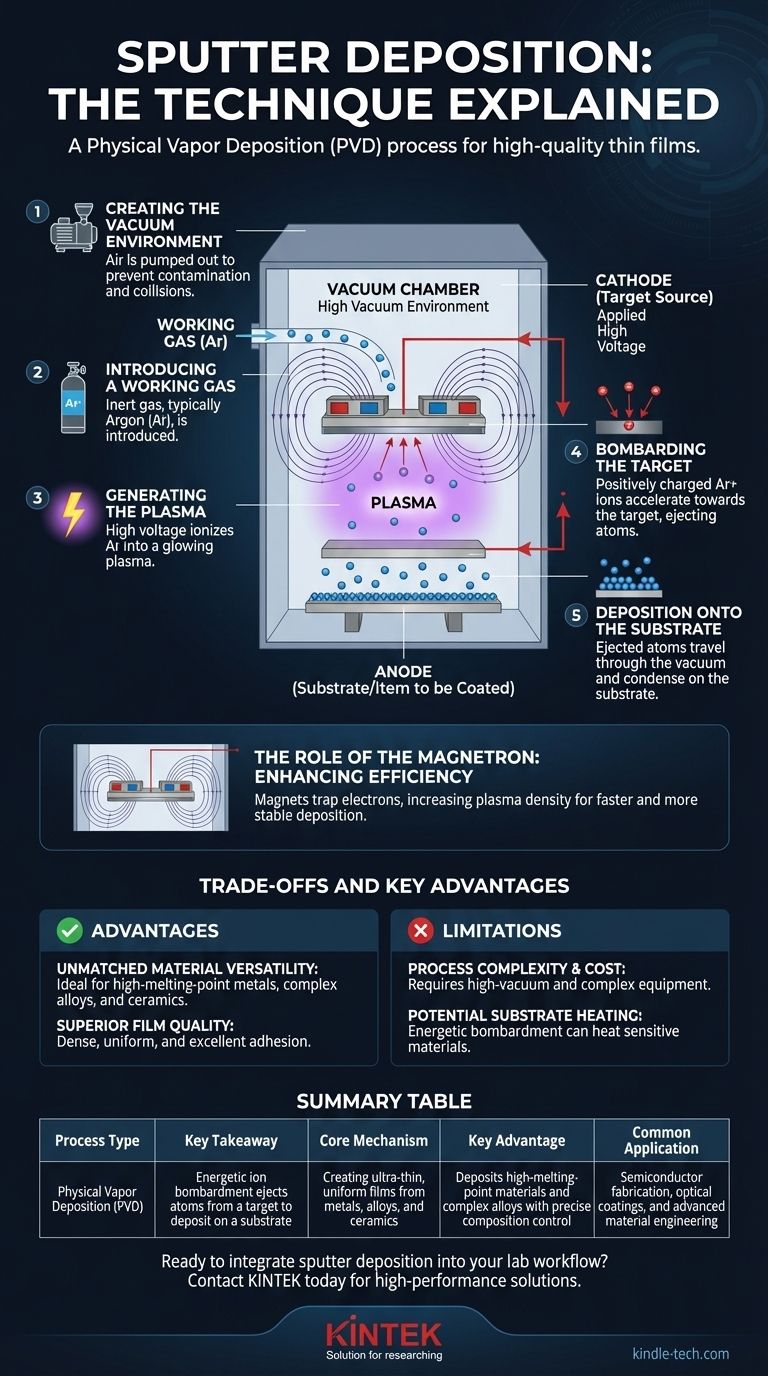
The Core Mechanism: From Plasma to Film
Sputtering is a step-by-step process that takes place entirely within a sealed vacuum chamber. Each step is critical for producing a high-quality, uniform thin film.
Step 1: Creating the Vacuum Environment
The entire process begins by pumping all the air out of a chamber to create a high vacuum. This is crucial to prevent the sputtered atoms from colliding with air molecules and to avoid contaminating the final film.
Step 2: Introducing a Working Gas
Once a vacuum is established, a small, precisely controlled amount of an inert gas—most commonly Argon (Ar)—is introduced into the chamber. This gas will become the source of the "sandblasting" particles.
Step 3: Generating the Plasma
A high voltage is applied between two electrodes inside the chamber: a negatively charged cathode (which holds the source material, or "target") and a grounded anode (which holds the item to be coated, or "substrate"). This voltage ignites the argon gas, stripping electrons from the argon atoms and creating a glowing, ionized gas known as a plasma.
Step 4: Bombarding the Target
The positively charged argon ions within the plasma are strongly attracted to the negatively charged target. They accelerate towards the target and strike its surface with significant kinetic energy.
This high-energy impact physically dislodges, or "sputters," atoms from the target material, ejecting them into the vacuum environment.
Step 5: Deposition onto the Substrate
The freed atoms from the target travel through the vacuum chamber until they strike the substrate. Upon arrival, they condense and bond to the surface, gradually building up a thin film of the target material.
The Role of the Magnetron: Enhancing Efficiency
Modern sputtering systems almost always use magnets to improve the process, a technique known as magnetron sputtering.
Why Basic Sputtering Isn't Enough
In a simple system, the plasma is not very dense, and the process of creating ions is inefficient. This leads to slow deposition rates and can cause excessive heating of the substrate.
Trapping Electrons with Magnets
To solve this, powerful magnets are placed behind the target. The magnetic field traps the free electrons from the plasma in a tight, looping path directly in front of the target's surface.
The Result: A Denser Plasma and Faster Deposition
These trapped electrons spiral around the magnetic field lines, dramatically increasing their chances of colliding with and ionizing neutral argon atoms. This creates a much denser, more localized plasma, which generates more ions to bombard the target. The result is a significantly faster and more stable deposition rate.
Understanding the Trade-offs and Key Advantages
Sputtering is a powerful technique, but it's essential to understand its specific strengths and limitations compared to other deposition methods.
Advantage: Unmatched Material Versatility
Because sputtering is a physical process, not a chemical or thermal one, it can be used to deposit almost any material. It is especially effective for materials with extremely high melting points (refractory metals) and for creating films from complex alloys whose composition must be precisely maintained.
Advantage: Superior Film Quality
The sputtered atoms arrive at the substrate with considerable energy. This results in films that are typically very dense, uniform, and have excellent adhesion to the substrate surface.
Limitation: Process Complexity and Cost
Sputtering systems require high-vacuum equipment, high-voltage power supplies, and often complex magnetron assemblies. This makes the equipment more expensive and complex than some alternatives, like simple thermal evaporation.
Limitation: Potential for Substrate Heating
The constant bombardment of energetic particles (ions, electrons, and sputtered atoms) can transfer a significant amount of energy to the substrate, causing it to heat up. This can be a concern when coating temperature-sensitive materials like plastics.
Making the Right Choice for Your Goal
Sputter deposition is not a one-size-fits-all solution. Your specific goal determines whether it is the right process for your application.
- If your primary focus is depositing complex alloys or refractory metals: Sputtering is the superior choice because it bypasses melting point limitations and preserves the material's original composition.
- If your primary focus is achieving a dense, uniform, and well-adhered film: The energetic nature of the sputtered atoms provides excellent film quality that is difficult to achieve with other methods.
- If your primary focus is rapid coating of simple, low-melting-point materials: You might consider thermal evaporation as a faster and potentially lower-cost alternative, though sputtering offers greater control.
By understanding its principles, you can leverage sputter deposition as a foundational tool for advanced material engineering and semiconductor fabrication.
Summary Table:
| Aspect | Key Takeaway |
|---|---|
| Process Type | Physical Vapor Deposition (PVD) |
| Core Mechanism | Energetic ion bombardment ejects atoms from a target to deposit on a substrate |
| Primary Use | Creating ultra-thin, uniform films from metals, alloys, and ceramics |
| Key Advantage | Deposits high-melting-point materials and complex alloys with precise composition control |
| Common Application | Semiconductor fabrication, optical coatings, and advanced material engineering |
Ready to integrate sputter deposition into your lab workflow? KINTEK specializes in high-performance lab equipment and consumables, including advanced sputtering systems designed for precision and reliability. Whether you're working with complex alloys, ceramics, or temperature-sensitive substrates, our solutions ensure superior film quality and process control. Contact us today to discuss your specific coating needs and discover how KINTEK can enhance your research or production capabilities.
Visual Guide
Related Products
- Tungsten Evaporation Boat for Thin Film Deposition
- Chemical Vapor Deposition CVD Equipment System Chamber Slide PECVD Tube Furnace with Liquid Gasifier PECVD Machine
- Custom CVD Diamond Coating for Lab Applications
- Customer Made Versatile CVD Tube Furnace Chemical Vapor Deposition Chamber System Equipment
- Evaporation Boat for Organic Matter
People Also Ask
- What is a thin film evaporator? A Gentle Solution for Heat-Sensitive & Viscous Materials
- What is the source of evaporation for thin film? Choosing Between Thermal and E-Beam Methods
- What methods are used to deposit thin films? A Guide to PVD, CVD, and ALD Techniques
- What is the process of thin film deposition? A Guide to PVD, CVD, and Coating Techniques
- What are the two primary categories of deposition technologies? PVD vs. CVD Explained


