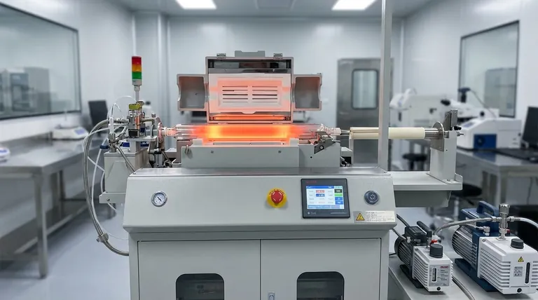
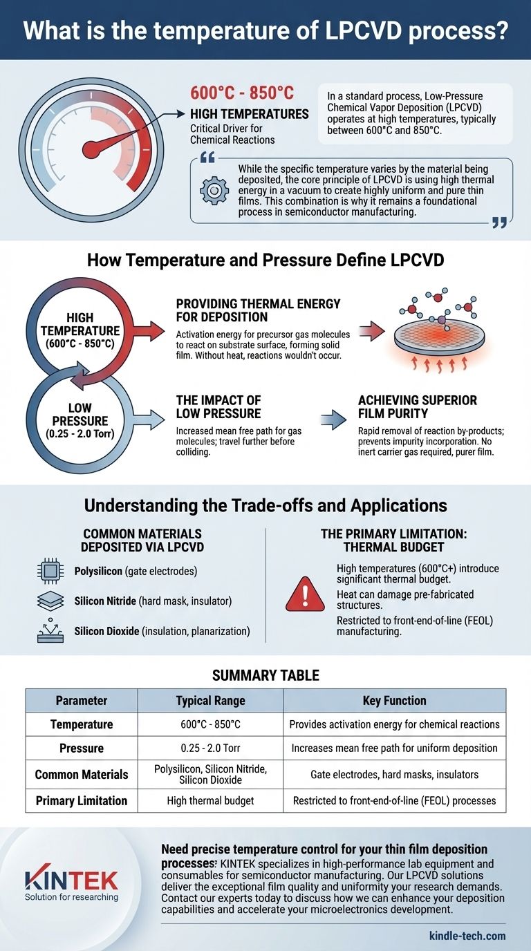
In a standard process, Low-Pressure Chemical Vapor Deposition (LPCVD) operates at high temperatures, typically between 600°C and 850°C. This thermal energy is the critical driver for the chemical reactions that deposit thin films onto a substrate, while the low-pressure environment is essential for achieving exceptional film quality and uniformity across the wafer.
While the specific temperature varies by the material being deposited, the core principle of LPCVD is using high thermal energy in a vacuum to create highly uniform and pure thin films. This combination is why it remains a foundational process in semiconductor manufacturing.
How Temperature and Pressure Define LPCVD
The high-temperature, low-pressure environment is not arbitrary; it is engineered to solve specific challenges in thin film deposition. These two parameters work together to create ideal conditions for building high-quality material layers.
Providing Thermal Energy for Deposition
LPCVD is a thermally-driven process. The high temperatures within the reaction chamber provide the necessary activation energy for precursor gas molecules to react on the substrate surface, forming the desired solid film.
Without sufficient heat, these chemical reactions would not occur at a practical rate, if at all. The temperature is carefully controlled based on the specific material being deposited, such as polysilicon, silicon nitride, or silicon dioxide.
The Impact of Low Pressure
The process operates under a vacuum, typically between 0.25 and 2.0 Torr. This low-pressure environment dramatically increases the mean free path of gas molecules, meaning they can travel farther before colliding with each other.
This increased travel distance is the key to LPCVD's superior results. It allows the precursor gases to diffuse evenly across the entire wafer surface and deep into complex structures like trenches, leading to highly uniform and conformal films.
Achieving Superior Film Purity
The vacuum system also allows for the rapid removal of reaction by-products from the chamber. This prevents these unwanted molecules from being incorporated into the growing film as impurities.
Furthermore, unlike atmospheric pressure processes (APCVD), LPCVD does not require an inert carrier gas (like nitrogen or argon). This eliminates a potential source of contamination, resulting in a purer deposited film.
Understanding the Trade-offs and Applications
LPCVD is a powerful and precise technique, but its high operating temperature creates a significant trade-off that dictates where it can be used in the semiconductor fabrication sequence.
Common Materials Deposited via LPCVD
LPCVD is the workhorse for depositing several fundamental films in microelectronics due to its excellent quality and conformality.
Key materials include:
- Polysilicon: Used for creating the gate electrodes in transistors.
- Silicon Nitride (Si₃N₄): Serves as a hard mask, an encapsulation layer, or an insulator.
- Silicon Dioxide (SiO₂): Used for insulation (dielectrics) and planarization.
The Primary Limitation: Thermal Budget
The high temperatures of LPCVD (600°C+) introduce a significant thermal budget. This means the process exposes the wafer to a large amount of heat for a sustained period.
This heat can damage or alter structures that have already been fabricated, such as low-melting-point metal interconnects. Consequently, LPCVD is typically restricted to the front-end-of-line (FEOL) manufacturing steps, before temperature-sensitive components are created.
How to Apply This to Your Project
Your choice of a deposition method depends entirely on the film requirements and the constraints of your fabrication process.
- If your primary focus is film quality and uniformity: LPCVD is the superior choice for applications where conformality and low defect density are critical, such as for gate polysilicon or trench isolation dielectrics.
- If your primary focus is processing temperature-sensitive devices: You must consider lower-temperature alternatives like Plasma-Enhanced CVD (PECVD), which sacrifices some film quality for the ability to deposit on completed device structures.
Understanding the role of temperature in LPCVD empowers you to leverage its strengths for creating high-performance microelectronic devices.
Summary Table:
| LPCVD Parameter | Typical Range | Key Function |
|---|---|---|
| Temperature | 600°C - 850°C | Provides activation energy for chemical reactions |
| Pressure | 0.25 - 2.0 Torr | Increases mean free path for uniform deposition |
| Common Materials | Polysilicon, Silicon Nitride, Silicon Dioxide | Gate electrodes, hard masks, insulators |
| Primary Limitation | High thermal budget | Restricted to front-end-of-line (FEOL) processes |
Need precise temperature control for your thin film deposition processes? KINTEK specializes in high-performance lab equipment and consumables for semiconductor manufacturing. Our LPCVD solutions deliver the exceptional film quality and uniformity your research demands. Contact our experts today to discuss how we can enhance your deposition capabilities and accelerate your microelectronics development.
Visual Guide
Related Products
- Inclined Rotary Plasma Enhanced Chemical Vapor Deposition PECVD Equipment Tube Furnace Machine
- Inclined Rotary Plasma Enhanced Chemical Vapor Deposition PECVD Equipment Tube Furnace Machine
- Chemical Vapor Deposition CVD Equipment System Chamber Slide PECVD Tube Furnace with Liquid Gasifier PECVD Machine
- Laboratory CVD Boron Doped Diamond Materials
- Microwave Plasma Chemical Vapor Deposition MPCVD Machine System Reactor for Lab and Diamond Growth
People Also Ask
- What is the necessity of depositing a silicon nitride (SiNx) thin film using PECVD? Optimize QSSPC Lifetime Measurement
- How does the PECVD function enhance thin-film properties? Achieve Superior Chemical Stability & Durability
- What is plasma enhanced chemical vapor deposition PECVD equipment? A Guide to Low-Temperature Thin Film Deposition
- What is Plasma Enhanced Chemical Vapor Deposition (PECVD)? High-Quality Film Deposition at Low Temperatures
- What is plasma activated chemical vapour deposition method? A Low-Temperature Solution for Advanced Coatings


